


NIMS Facilities
MANA researchers will be able to use many of NIMS's world-renowned facilities, beginning with advanced medium- and large-scale devices.
MANA Foundry
At MANA Foundry Station, we provide the facilities which can use the forefrontive core-technique for materials science researchers who utilize nanotechnology in Japan.
Nano Quantum Foundry is a nano-fabrication center for researches of nanomaterials and nanodevices.There are engineering staffs to support the researchers.
Beam Line
At Beam Station, we are providing a lot of opportunities to the users to access a contract beamline NIMS-BLI5XU(Wide Energy range Beamline for research in Advanced Materials(WEBRAM)) at SPring-8.
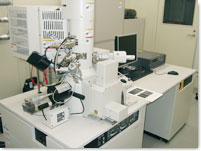
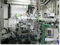
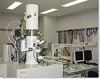
High Voltage Electron Microscope
The High Voltage Electron Microscopy Station (HVEMS) has been established for the research and development (R&D) of HVEMs and related instrumentation for nano-characterization and study of material systems, and for utilization by users including those who are not specialists of TEM. The focus of the R&D is the dynamic observation of materials on the atomic scale, improvement in spatial resolution, advanced spectroscopic characterization of materials and, development of systems for remote operation and so on.
Belt type High Pressure (HP) Apparatus
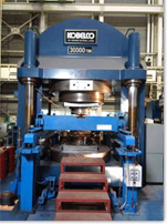
Belt type HP apparatus
- Contact Researcher;
- Takashi Taniguchi
Materials synthesis and treatment under high pressure and high temperature.
2000 ton Press : 2 - 10 GPa, 2000°C sample volume: ~1.5 cc.
30000 ton Press: 2 - 6 GPa, 3000°C sample volume: ~7 cc.
- Building:
- Extreme Technology laboratory, Room:101, Namiki Site
High energy X-ray photoemission spectroscopy
High energy X-ray photoemission spectroscopy and schematic diagram of X-ray optics
- Contact Researcher;
- Hideki Yoshikawa
- Specification
- Maximum analyzing energy of photoelectrons is 6 keV. Energy resolution reaches 60 meV under the condition that 6 keV X-rays are monochromatized by Si(333) channel-cut-crystal.
- Installation location
- SPring-8 NIMS beamline BL15XU
- Potential
- Owing to long observation depth, high energy XPS is powerful to clarify the electronic structure and chemical bonding of functional devices which have nano-meter-sized layer structures. Moreover, high-resolution valence-band-analysis enables to evaluate the energy level of carriers in electron devices.
High precision powder X-ray diffractometer
High precision powder diffractometer
- Contact Researcher;
- Hideki Yoshikawa
- Specification
- Combination of the imaging plate detector and high-brilliant synchrotron radiation X-rays realizes the high precision diffraction pattern of which angular width is 0.003 degree.
- Installation location
- SPring-8 NIMS beamline BL15XU
- Potential
- Owing to high throughput measurement, high precision powder X-ray diffractometer with imaging plates is quite useful not only for the structural analysis of complex materials but also for the analysis of the phase transition induced by light illumination, temperature change, electric field, and so on.
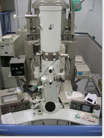
Dual-ion beam interfaced high-voltage electron microscope; Accelerating voltage : 1000 kV
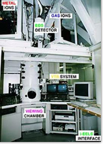
High precision powder diffractometer
- Contact Researcher;
- Kazutaka Mitsuishi at Sakura site
Ultrahigh resolution objective lens : Cs = 2.6 mm, Cc = 3.4 mm
Point resolution : 0.13 nm, Lattice resolution : 0.10 nm
(Capability of dymanic observation with atomic resolution)
High vacuum : below 3×10⁻⁶ Pa around specimen stage
Eucentric side entry stage : more than 40 degree tilt
Heating and cooling : from 10 K to 1073 K
Beam spot : smaller than 10 nm at 400 keV operation
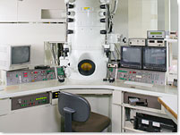
Ultrahigh-vacuum transmission electron microscope
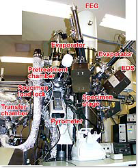
High precision powder diffractometer
- Contact Researcher;
- Kazutaka Mitsuish iat Sakura site
Ultrahigh resolution objective lens (Cs = 0.7 mm, Cc = 1.2 mm)
Point resolution 0.21 nm & Lattice resolution 0.10 nm
Ultrahigh vacuum below 3×10⁻⁸ Pa around specimen stage
ZrO/W Schottkey FEG providing the fine prove below 0.5 nm in diameter & small energy dispersion about 0.8 eV for EELS
UHV Energy dispersive X-ray spectrometer (UHV EDS)
Pretreatment chamber in which preheating, Deposition, Gas reaction etc. is carried out Cartridge type TEM specimen holders
(Double tilt furnace heating holder, Double tiit resistative heating holder, Single tilt resistative heating holder, Double tilt holder, Single tilt holder)
Dedicated scanning transmission electron microscope; Accelerating voltage : 200 kV
High precision powder diffractometer
- Contact Researcher;
- Kazutaka Mitsuishi at Sakura site
Resolution : TEM(Lattice image) 0.14 nm, STEM(lattice image) 0.2 nm, SEI 1.0 nm
Easy operation based on Windows GUI control. BF/DF-STEM, SEI , TEM and SAD are observable.
STEM-EELS is available.
Preliminal observation transmission electron microscope
High precision powder diffractometer
- Contact Researcher;
- Kazutaka Mitsuishi at Sakura site
- Acc voltage : (100 keV,200 keV),300 keV
- Resolution : Point resolution 0.17 nm, lattice resolution 0.10 nm
- Recording :
- Multi-scan CCD camera(2k × 2k), imaging plate (IP), video and negative film
- Capability :
-
- High-resolution transmittion electron microscopy(HRTEM)
- Nano-beam electron diffraction(NBED)
- Energy dispersive X-ray spectroscopy(EDS)
- Electron energy loss spectroscopy(EELS) & energy filter imaging(EFI)
- Electron holography
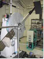
Tsukuba Magnet Laboratory
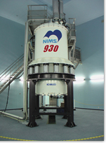
930MHz NMR Magnet
Field: 21.6 T , Bore 54 mm
H Probe HCN Probe
Homogeneity: < 0.1 ppm/10 mmΦ × 20 mm
SoftMaterial Line
- Contact Researcher;
- Nobutaka Hanagata at Sengen site
- Adjustment of Biomoleculars
- Bio-imaging laboratory
- Cell Culture test
- Instrumental Analysis
- Synthesis of Organic and Polymer Materials
Here, we can show the selected instruments.
Laser-capturer Microdissection System (LMD6000 MPP)
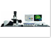
Confocal Laser Microscope (TCS SP5)
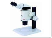
Stereomicroscope including digital camera (MZ16+DFC290, S8 APO+EC3)
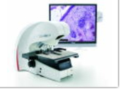
Digital Microscope (DMD108)
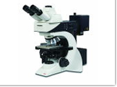
Erecting Fluorescence Microscope (DM2500 Fluo/DIC)
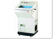
Freezing Microtome (CM1850)
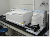
Fourier Transform Raman spectroscopy (SPECTRUM GX-Raman)
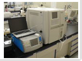
GPC with MALLS (GPC101)
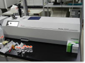
Zeta-potential & particle size analyzer (DELSA 440SX)