Development and Application of Material Evaluation Methods Using Transmission Electron Microscopy (TEM)

Transmission electron microscopy (TEM) enables various types of microstructural analysis, such as imaging for observing magnified images of ultra-small regions, crystal structure analysis via electron diffraction patterns, and elemental analysis using techniques like electron energy loss spectroscopy (EELS). With advancements such as aberration correctors, monochromators, and highly sensitive detectors, it has become possible to evaluate and analyze materials at atomic resolution. We have developed TEM techniques and data analysis methods for high-precision and high-sensitivity measurements, including extraction of useful information from large-scale data obtained by methods such as 4D-STEM through unsupervised machine learning (dimensionality reduction and clustering). By combining a variety of TEM methods to evaluate microstructures that realize unique physical properties or superior performance, we aim to contribute to strengthening innovation in materials science. Please see details here.


Details  

TEM-Based Nanoscale Thermal Transport Measurement Using Electron Beam Pulses

To achieve precise material design and device development for advanced heat dissipation materials, thermal insulators, and thermoelectric materials, it is essential to directly observe how phonons are scattered and how much thermal resistance arises in local regions such as defects and interfaces, and to understand the phenomena involved in thermal transport. We are developing a new thermal transport evaluation method based on TEM that allows for the direct nanoscale measurement of thermal transport while simultaneously observing microstructures. In particular, by pulsing the electron beam, we focus on developing methods for quantitative measurement of the thermal diffusivity of TEM specimens based on phase and amplitude analysis of thermal waves, as well as time-resolved in situ observation of thermal waves.


Molecular Electron Microscopy for Chemistry

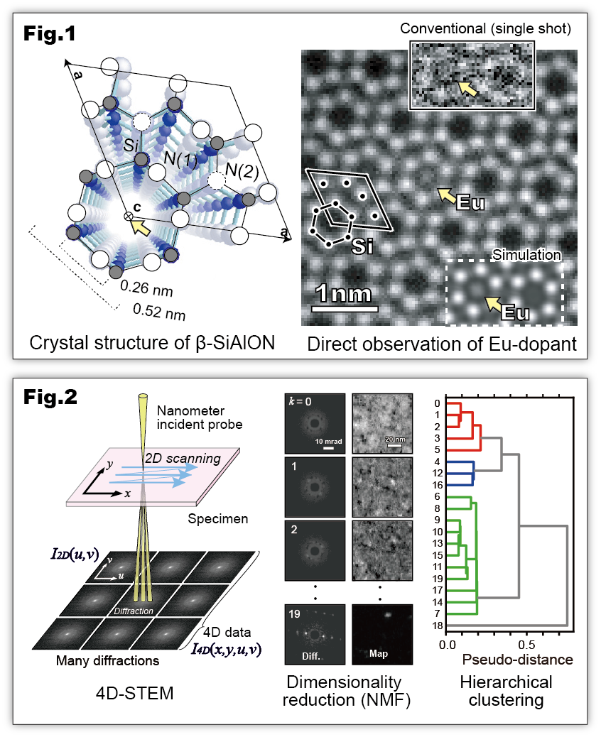
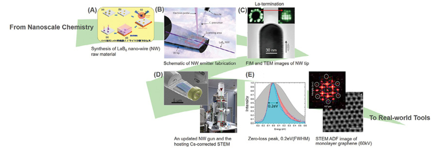
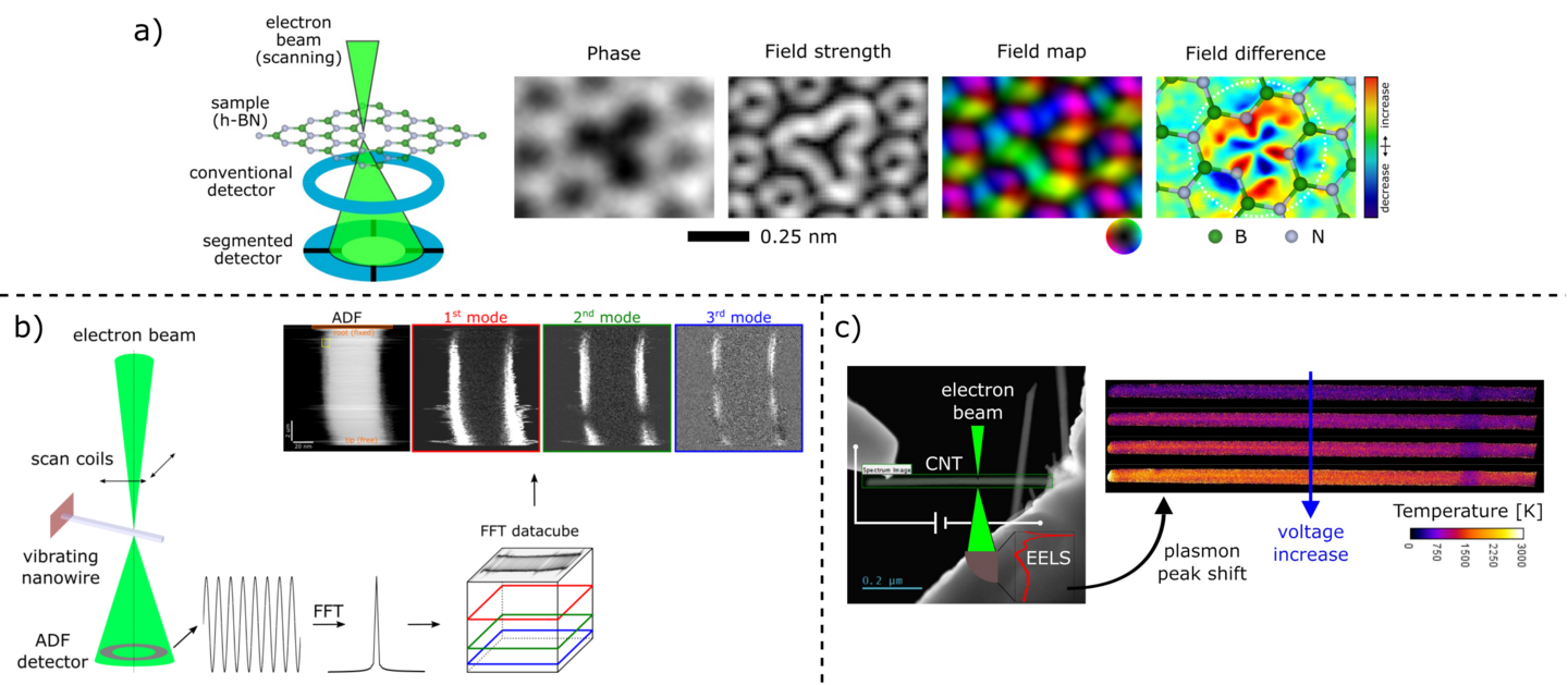
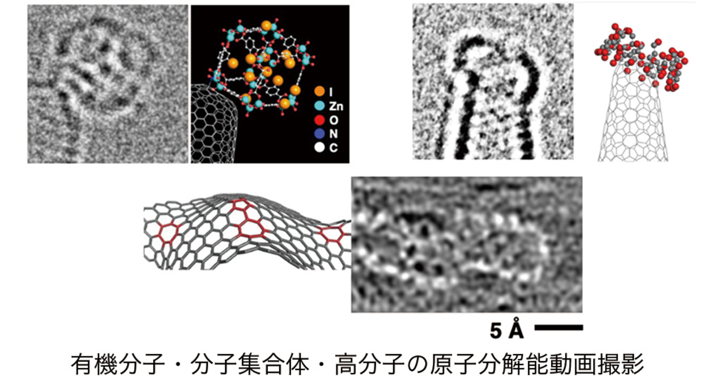
In the electron microscopy observation of molecular materials such as molecular assemblies, organic and coordination compounds, and polymers, sample damage caused by electron beam irradiation has hindered high-resolution imaging. We are advancing "cinematic molecular science" by clarifying the structures of single molecules and molecular assemblies at atomic resolution, and by recording dynamic processes involving molecules—such as chemical reactions and structural transformations—in real-time video, using our uniquely developed sample preparation methods and high-speed electron microscopy video recording and analysis techniques. Furthermore, by leveraging the electron microscopy technologies cultivated in these studies, we are working on the development of functional molecular assembly materials, such as nanometer-thick films, based on an understanding of the hierarchical molecular assembly mechanisms in the nano- and meso-scale regions that bridge the molecular and macroscopic worlds.

Development and Application of Electron Energy Loss Spectroscopy (EELS) Measurement Techniques

There is a growing demand for technologies capable of high-precision measurements of various physical properties at nanometer resolution. We are developing and applying STEM-EELS, a technique that combines ultra-high energy resolution EELS (approximately 20 meV) with scanning transmission electron microscopy (STEM) to enable the measurement of physical properties in the infrared region at nanometer-scale resolution. Specifically, by achieving ultra-high energy resolution (~20 meV), spatial resolution (~1 nm), and wavenumber resolution (~3 nm-1) with STEM-EELS, it is possible to precisely measure the physical properties in the infrared region at nanometer resolution.


Next-Generation Electron Microscopy Using LaB6 Nanowire Cold Field Emission

Cold field emission (CFE) produces the brightest and the most monochromatic electron beam. Such electron beam is highly demanded in application of electron microscopy for use in material research, pharmaceutic discovery and semiconductor manufacturing. For a long time, wide application of CFE was hindered because it suffers from emission instability in conventional vacuum condition. We produced nanowires of LaB6 material one out of 100 billion size of a conventional electron emitter. The combination of low work function and nanometric size produced an emission brightness 100 times higher and stability 10 times better than conventional electron sources. Wide application of LaB6 nanowire CFE has been realized from compact tabletop SEMs to atomic-resolution aberration-corrected TEMs.

Novel Microscopy Techniques for Advanced Characterization

Our aim is to extend the range of information that can be obtained by TEM by developing new analysis methods. By combining these new techniques with the already impressive capabilities of modern TEMs, we can measure material properties which are not accessible by any other methods. This furthers our understanding of the advanced materials investigated and provides feedback towards improving their performance.
• Atomic-resolution measurement of the distribution of electric fields around defects in 2-D materials
• Direct observation of the thermal vibration modes of individual nanowires
• Nanometer-scale temperature mapping of in-situ Joule-heated carbon nanotubes