Back to Group Research>
To Japanese contents>
Transmission electron microscopy encompasses imaging, diffractometry, and spectroscopy techniques, enabling a variety of materials characterizations. This website describes the electron microscopy research and materials evaluation conducted mainly on Electron Microscopy Group.
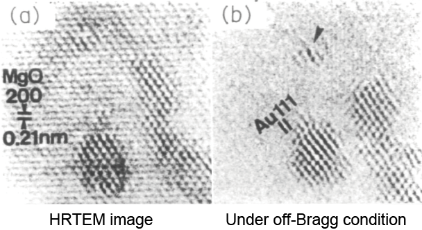
Using an ultra-high-voltage electron microscope (accelerating voltage 1 MeV), we observed Au nanoparticles embedded in single-crystal MgO. To avoid lattice fringes of the MgO crystal, we intentionally tilted the specimen from the crystal plane axis, i.e., off-Bragg condition, and observed clusters consisting of a few Au atoms (Electron Microscopy Society of Japan Paper Award (1992). This work was supervised by Prof. Nobuo Tanaka and Prof. Kazuhiro Mihama) [JEM 1989].
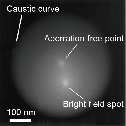
Axial coma aberration limits the resolution of HRTEM, but it cannot be measured by a Fourier transform of a single TEM image. We proposed a method for align the coma-free axis using a single defocused image [Ultramicroscopy 2003]. The proposed method utilizes a specimen as an amplitude-splitting beam splitter, and employs caustic figures caused by the spherical aberration of the objective lens. It is theoretically equivalent to the Ronchigram alignment for STEM.
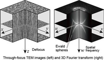
We proposed a method to quantitatively determine spatial resolution (information limit) by performing a 3D Fourier transform of through-focus (continuously varied focus) TEM images. The Young's fringe method, which is still used, cannot accurately evaluate spatial resolution due to nonlinear imaging terms.The principle is based on “active image processing” proposed by Profs. Ikuta, Shimizu, Takai, and Taniguchi before the 1990s. We performed through-focus image measurement, drift correction, and 3D Fourier transform using a custom DigitalMicrograph scripts. We determined the spatial resolution of low-acceleration electron microscopes and monochromator TEMs. [Ultramicroscopy 2012], [Ultramicroscopy 2013].
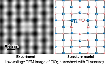
We applied high-resolution low-voltage TEM to the observation of TiO2 nanosheets synthesized by Dr. Sasaki (NIMS). Using monochromated TEM @80kV, we directly observed Ti atomic defects of TiO2 nanosheet [Sci.Rep.2013]. We also demonstrated that TiO2 nanosheets can be topotactically reduced as Ti2O3 nanosheets due to beam irradiation [JCPL 2011].
We have been using various cameras for electron microscopy (MultiScan CCD, UltraScan CCD, OneView, RIO), and the sensitivity coefficients (conversion efficiencies) of the cameras were experimentally calibrated by us. The conversion efficiencies vary depending on the device and acceleration voltage. Our experimental setup includes the DigitalMicrograph script that adjusts the sensitivity coefficient, and the camera intensity is always converted to the number of electrons. Electron probe current can also be measured down to the sub-picoampere range.
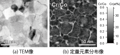
We combined a Gatan Energy Filter (GIF 678) with a field emission TEM (HF-2000) in 1994, and demonstrated EFTEM elemental mapping with a spatial resolution of 1 nm [JJAP1994], [JM 1995]. EFTEM mapping was also applied to the observation of semiconductor devices (Japanese Applied-Physics Award for young researchers (1997)). Subsequently, based on requests from material scientists, we first quantitatively observed elemental mapping, which was previously only qualitative. In the observation of magnetic recording media CoCr, we clarified the correlation between magnetic properties (e.g., coercive force) and substrate temperature from quantitative elemental mapping [JJAP 1995]. This is because magnetic properties can be determined from the Slater-Poling curve once the Cr composition is known. We also observed Cr-depleted zone in stainless steel after sensitization treatment [JEM 1996]. In stainless steel, corrosion resistance decreases when the Cr composition drops below approximately 10%, making the quantitative value of Cr composition crucial.
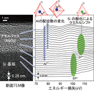
By adjusting the focus of an EEL spectrometer, a technique that allows simultaneous measurement of spectra at multiple positions was called spatially-resolved EELS [JEM 1997]. This method is a real-space adaptation of the anglular-resolved EELS performed by Dr. Hiroshi Watanabe (Hitachi) in the 1960s using a Moellenstedt spectrometer. We accurately measured the chemical shifts of Si L-shell and K-shell, as well as the chemical shifts of SiO₂/SiN/SiON/Si substrates fabricated using semiconductor processes [Microscopy 2001]. In the Semiconductor MIRAI Project, we analyzed the change in the coordination number of Al near the Al₂O₃/Si interface using spatially-resolved EELS[APL 2003]. The first-principles calculations of EEL spectra for Al with 4- and 6-coordination were provided by Prof. Mizoguchi and Prof. Isao Tanaka.
Since spatially-resolved EELS can simultaneously measure electrons at different energies, we used this method to discuss the delocalization and interference of inelastic scattered electron [Ultramicroscopy 2003]. At the time, when I presented the finding that “inelastic scattered electrons interfere,” Pro. Michiyoshi Tanaka asked an insightful question. From this point on, I realized that achieving atomic resolution with EFTEM was theoretically challenging and began preparing for STEM.
We successfully decomposed and mapped atomic columns for the first time using STEM-EELS [Nature 2007]. It is crucial to utilize inner-shell excitation processes where inelastic scattering is localized. We demonstrated that La-atomic colmns is invisible in N-shell excitation but visible in M-shell excitation. At energy losses of several hundred eV, the delocalization factor limits spatial resolution. Si L-shell excitation (~100 eV) is highly delocalized, and atomic columns in the crystal are inherently indistinguishable. Interference fringes do not correspond to actual elemental distributions.
Note that Even in the case of Si L-shell excitation, atomic columns can be resolved by increasing the energy loss value (i.e., EXELFS range) [Micron 2008].

The apparatus used in the experiment was a Hitachi STEM dedicated instrument (HD-2300C) that had been thoroughly modified. When it was presented at a conference, its transformed appearance [Microscopy 2007] caused Hitachi salesperson confused. We are deeply grateful to Drs. Isakozawa, Nakamura, Soda, and Kato of Hitachi. Prof. Suenaga encouraged me to submit the paper to Nature.
In December 2010, our group finally introduced aberration-corrected STEM/TEM with a monochromator, and Dr. Haruta reported atomic resolution mapping of chemical bonding states [APL 2012], Dr. J. Kikkawa reported Li maps of lithium battery cathodes [JPCC 2015], and Dr. Nagai reported mapping of Bi-based high-temperature superconductors [Physica C 2014]
The energy resolution of EELS is determined by the energy spread of the zero-loss peak and the energy instability (e.g., acceleration voltage). To improve the energy resolution of the 300 kV cold field emission gun (CFEG), we modifed the apparatus in hardware and software. We attached shielding box for the high-voltage power supply. When Dr. Krivanek visited NIMS in the early 2000s, he knocked on our high-voltage tank to check for fluctuations in the accelerating voltage. Due to various reasons, the zero loss peak fluctuated, causing the energy resolution to deteriorate during long measurements. To address this, we developed software that performs high-speed multiple measurements and corrects drift after measurement. We implemented triple exposure in the order of low-loss, high-loss, and low-loss, followed by simultaneous readout, improving the effective energy resolution and accuracy of EELS[J.Microsc. 2002]. A similar concept is currently commercialized as DualEELS by Gatan Inc.
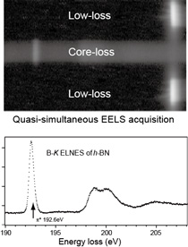
By measuring low-loss before and after core-loss, drift and instability are suppressed, enabling EELS measurements with high energy accuracy and effective high energy resolution.
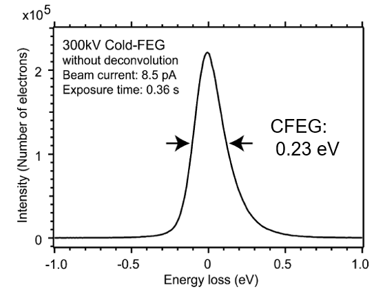
Furthermore, by acquiring spectra with the shutter open during full-frame CCD readout —a method known as streak imaging— we achieved the highest resolution of 0.23 eV with CFEG. We experimentally clarified that the energy resolution of CFEG is physically determined by the Fermi tail and tunneling tail. Micron 2005.
If low-loss and high-loss spectra can be measured simultaneously, the low-loss spectrum can be used as an instrument function, and the high-loss spectrum can be deconvolved. Dr. Ishizuka developed a deconvolution program using the Maximum-Entropy method and the Richardson-Lucy method[Microscopy 2003], which enabled us to discuss the fine structure of the spectrum. He also devised an algorithm to accelerate convergence, which has been commercialized as DeConvEELS (HREM Research Inc.).
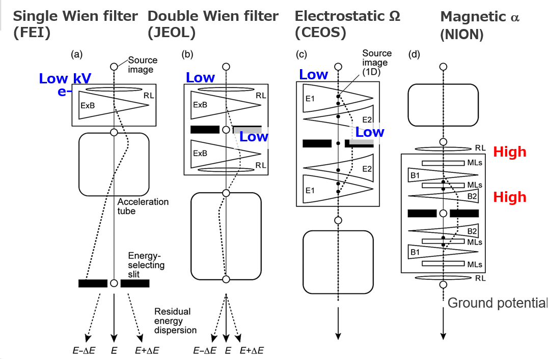
To achieve energy resolution of 0.2 eV or less, a monochromator is necessary. The first monochromator for electron microscopes was commercialized by FEI in 2001. Fortunately, in 2002, thanks to the kindness of Prof. Hofer, I had the opportunity to use the first unit in Graz, Austria, for a week, where I conducted experiments with Drs. Kothleitner and Grogger, who were of the same generation (I also attempted alignment operations, but that data was completely useless). Prof. Hofer introduced me to Dr. Schaffer, who was creating a database of DigitalMicrograph scripts.

At the time, the energy resolution of the monochromator was 0.2 eV (full-width at half maximum), which was not significantly different from the 0.23 eV of CFEG. However, monochromator did not exhibit the tunneling tail that is unavoidable in CFEG, and this was clearly evident when the zero-loss peak intensity was displayed on a logarithmic scale. This demonstrated the advantage of the monochromator and its suitability for band gap measurement. I reported that 1/1000 of the peak intensity should be used as an indicator of resolution[Micron 2005]. This value is unexpectedly called as Kimoto Limit (sometime). The comparison diagram with CFEG was also cited in the textbook by D.B.Williams & C.B.Carter. Following FEI's product announcement, JEOL, CEOS, and NION also commercialized monochromators. I reviewed those monochromators with their schematic diagrams in Microscopy [Microscopy 2014]. The schematic diagram was also cited in Hawkes & Spence, Handbook of Microscopy (2019). For details, please refer to the related papers.[Microscopy 2014]
STEM enables various types of imaging such as annular dark-field (ADF), annular bright-field (ABF), and bright-field (BF) imagings for structural analysis. In particular, ADF images can be regarded as incoherent imaging and excel in interpretability. At the beginning, we did not have an aberration corrector nor a monochromator, so we sought to improve resolution by software. We hypothesized that incoherent imaging, like EELS, could reduce noise through multiple fast acquisition and improve resolution through deconvolution.
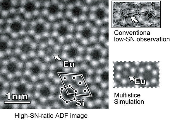
I therefore rewrote the script developed for EELS for use with STEM imaging. Through multiple measurements, we significantly improved the signal-to-noise ratio and succeeded in observing Eu single atoms in Eu-doped SiN [APL 2009]. In the observation of interstitial dopants, the channeling of incident electrons is important, and we also performed comparisons with simulations to identify the single dopant atom. This method was also applied to the observation of monolayer graphene [Microscopy 2015] and featured in Thermo Fisher's product catalog. Currently, high-speed multiple measurements are commercialized as DCFI in Velox (Thermo Fisher).
If the SN ratio is sufficiently high, the position of the bright spot in the ADF image can be determined with high precision, similar to the peak position in EELS. By deconvolving high-SN images using methods such as the Maximum Entropy method, the atomic position can be determined with precision far exceeding the resolution. By adding a tracking function to the mutiple fast acquisition software, we have improved the atomic position accuracy to the picometer order [Ultramicroscopy 2010].
Additionally, it has been pointed out that tilting the specimen reduces position accuracy and that bright spots may not correspond to atomic positions [JEM 2012]. From the perspective of whether the effort to achieve high "precision" measurements is truly "accurate" and meaningful (or, in other words, whether we are wasting time and money measuring something that is not worth measuring).
Our goal is to analyze crystal structures in nanometer regions. While ADF images excel in structural visualization, quantitative measurement of ADF image intensity is necessary for comparison with simulations. We accurately calibrated the nonlinear response of the ADF detection system and quantified the ADF image intensity [Microscopy 2015a]. Furthermore, by accurately quantifying the effective source on the sample, we have achieved graphene images with atomic resolution that match simulations at the quantum noise level and enable element identification [Microscopy 2015b]. We can also measure the brightness of the electron gun.

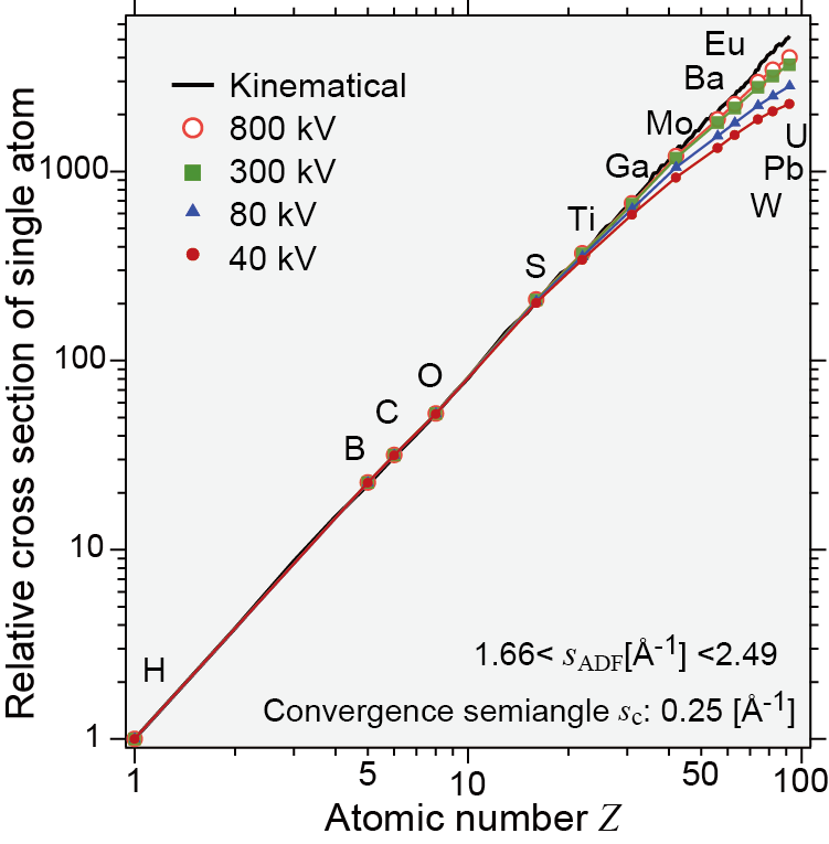
Next, we observed quantitative ADF images of MoS2 and WS2. ADF images are said to follow a power law proportional to 1.5 to 1.7 times the atomic number Z, but this law does not hold. Then we dynamically simulated single-atom ADF images using wave-optical methods and confirmed that they systematically deviate from the power-law relationship at low accelerating voltages and for heavy elements. [SciRep 2018]. This indicates that the first Born approximation breaks down even for single atoms in high angle scattering (i.e., thermal diffuse scattering).
When precise, accurate, and careful measurements yield results that differ from previous theories, they not only surprise us but also point us toward new research findings and directions.
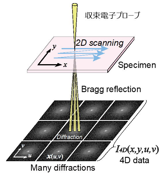
The technique of scanning an electron probe over a specimen in two dimensions while capturing diffraction patterns (2D) to obtain four-dimensional data was named 4D-STEM by Ophus in 2019. We first reported atomic resolution using this technique in 2011 [Ultramicroscopy 2011], although we named it spatially-resolved diffractometry at that time.
.png)
Furthermore, we treated the obtained measurement data as big data and combined 4D-STEM with unsupervised machine learning (dimensionality reduction and clustering) [Ultramicroscopy 2021], [Sci.Rep.2024], [Small Methods 2025]. While principal component analysis (PCA) is a widely known method for dimensionality reduction, we use nonnegative matrix factorization (NMF). While PCA is a representative method for feature extraction from multidimensional data, it has the issue that elements containing negative values cannot be interpreted as diffraction. On the other hand, NMF has high computational cost and may converge to local minima, but it provides interpretable results, making it suitable for experimental data analysis. We perform NMF calculations using a DigitalMicrograph script. We compare PCA while confirming computational load and convergence using the Alternating Least-Squares algorithm and the Multiplicative Update algorithm.
The factorized components obtained by NMF cannot always be interpreted as experimental results (diffraction and map), and it is known that artifacts can occur. To avoid artifacts by primitive NMF, we incorporated constraints into the ALS algorithm that prohibits intensity chges that are impossible for electron diffractions (constrained NMF) [Sci. Rep 2025]. As a result, it became possible to accurately separate crystalline precipitates from amorphous material.
With the advancement of scientific instruments, the amount of measurement data is expected to increase, and the integration of information science (i.e., informatics) with scientific instrument, i.e., Metrology Informatics or Measurement Informatics, is expected to progress further.
We are not at the forefront of information science. However, we do not believe that Metrology Informatics can be achieved simply by combining off-the-shelf software. It seems that domain-specific knowledge is also recognized as important in the field of information science.
For the cutting-edge Metrology Informatics in electron microscopy, we believe it is important to integrate knowledge of diffraction physics, electron optics, instrumentation, and materials science. Considering that one cannot be called a measurement expert without understanding the principles and instruments of measurement techniques, we aim to minimize the “black box” aspects of information science as much as possible. Regarding information science and software engineering, we plan to continue seeking guidance from experts or collaborating on research in the future.
We use DigitalMicrograph (DM) scripts for measurement and analysis using electron microscopes. For details, please see the [DM入門] although the contents are still in Japanese. Some English information about our DM scripts is available on GitHub kimotokoji/DMscripts.
We (Drs. Mitsuishi, Mitome, Hara, Nagai and Kimoto) have published a book titled “Transmission Electron Microscopy for Materials Research” (Kodansha, 2020) in Japanese.[TEM入門]
We would like to express our gratitude to our collaborators and advisors. We apologize for not being able to list all names (in no particular order and titles omitted). Kazuhiro Mihama, Nobuo Tanaka (Nagoya University), Michiyoshi Tanaka (Tohoku University), Yoshinori Tokura (University of Tokyo), Isao Tanaka (Kyoto University), Sigeto Isakozawa, Yoshifumi Taniguchi, Katsuhisa Usami, Tatsumi Hirano, Kazutosi Kaji, Kuniyasu Nakamura, Kohei Soda, Hiroshi Kato, Yotsuo Yahisa, Shinji Narishige, Masaaki Futamoto, Yoshiyuki Hirayama, Hiroyuki Hoshiya (Hitachi), Ryohei Matsumoto, Atsushi Suzuki (Thermo Fisher Scientific), Shigeo Horiuchi, Yoshio Matsui, Yoshio Bando, Chusei Tsuruta, Keiichi Yanagisawa, Takayoshi Sasaki, Takashi Taniguchi, Naoto Hirosaki, Jun Kikkawa, Koji Harano, Naoyuki Kawamoto, Han Zhang, Ovidiu Cretu, Takuro Nagai, Shinji Kohara, Atsushi Togo, Kazutaka Mitsuishi, Masayuki Mitome, Toru Hara, Keiji Kurashima, Megumi Ohwada, Mitsutaka Haruta (currently Kyoto University), Yoshihiro Nagao (currently Nagoya University), Shunsuke Yamashita (currently Sony), Shogo Koshikawa (currently JEOL), Mitsuhiro Saito (currently JEOL), Yeong-Gi So (currently Akita University), Toru Asaka (currently Nagoya Institute of Technology), Takumi Yoshimura, Masashi Uoda (DIC), Xiuzhen Yu (currently RIKEN), Akihiko Hirata (Waseda University), Motoki Shiga (Tohoku University), Yoshifumi Oshima, Kohei Aso (JAIST), Kenji Kaneko (Kyushu University), Koji Tanaka (AIST), Teppei Saeki, Koji Inoke, Koichi Takauchi (Gatan), Fumio Hosokawa (FH electron optics), Hiroshi Kageyama (Kyoto University), Kazuhiko Maeda (Science Tokyo), Ryo Ohtani (Kyushu University), Masami Terauchi (Tohoku University), Yuichi Ikuhara (University of Tokyo), Hiroki Kurata (Kyoto University), Kazu Suenaga (Osaka University), Teruyasu Mizoguchi (University of Tokyo), Kazuo Ishizuka, Akimitsu Ishizuka (HREM Research Inc.) O.L. Krivanek, R.F. Egerton, M. Malac, B. Freitag, E.v.Cappellen, S.Lazar, A.Bright, F. Hofer, G. Kothleitner, W. Grogger, C. Trevor, J. Hunt, M. Barfels, R. Twesten, M. Rabara, R.E. Dunin-Borkowski, et al.