")
Facilities
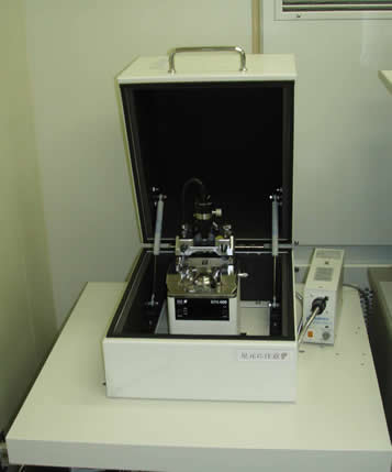
Surface structure analyzer system
MBE + RHEED + XPS + STM + XRD
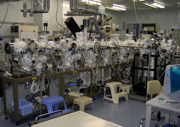
MOCVD system for As and P based materials
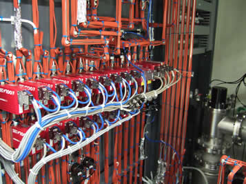
MOCVD system for nitrogen based materials
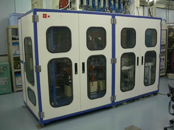
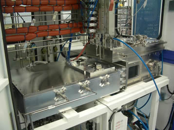
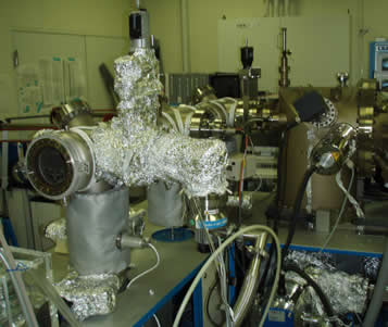
Molecular beam epitaxy system for oxide- and nitride- semiconductors. Sources: Zn, Mg, O-plasma, N-Plasma, Ga
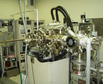
Molecular beam epitaxy system for III-Arsenide semiconductors. Sources: Al, Ga, In, As, Si, atomic-H
Mask aligner
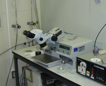
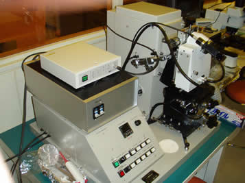
Wire bonder
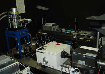
Photoluminescence measurement system
Lasers: 532 nm Nd-YAG laser (40 mW), 633 nm He-Ne laser (1mW), 325 nm He-Cd laser (20mW), Detectors: CCD camera (ANDOR), GaAs photomutiplier tube, InGaAs photomutiplier tube, Cryostat: Closed cycle cryostat (5 K-RT)
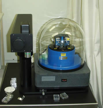
Atomic force microscope for lithography