
")
Fabrication of Semiconductor Quantum Nanostructures
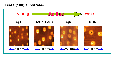
Our group is devoted to the development of GaAs QDs growth technique by using the droplet epitaxy, which was invented at NRIM, the former Institute of NIMS. Besides improving the optical quality of QDs, we have successfully made a variety of nanostructures including QD pairs and rings, and have clarified their optical and electronic properties. Recently, it was revealed that both the shape and the energy states of QDs can be tuned if they are grown on the higher index substrates. We analyze the growth surface with STM and RHEED to understand the formation mechanism of nanostructures and to control their growth at higher index surfaces. Our research group is also studying other quantum nanostructures such as droplet QDs of GaSb/GaAs system having type-II energy band and a novel approach using isoelectronic traps in III-V compound semiconductors. In addition, we study single-photon source, semiconductor laser diode using droplet QDs, and the epitaxial growth and the interface control of III-V on Si substrate.
Materials
![[PDF]](../img/pdficon_small.gif) Advancement of droplet epitaxy
Advancement of droplet epitaxy- GaAs quantum dot laser
- GaAs quantum dot pair
- Surface control for III-V MISFET
- Research on Semiconductor Nanostructures Exploited for Quantum Information and Communication Technology
- Atomistic control of surface and interface structures on compound semiconductors
- GaSb TypeII quantum dot