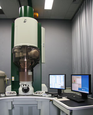
実動環境対応物理分析電子顕微鏡
Real Working Environment Physical Characterization TEM
JEM-ARM200F-G (JEOL)
照射レンズ系、結像レンズ系のそれぞれに収差補正機能を搭載し、超高分解能を実現すると共に、様々な実動作環境におけるその場観察・分析・ポテンシャル計測を可能にした透過形電子顕微鏡です。
This microscope has TEM image and STEM probe aberration correctors for high-resolution observations. Furthermore, it enables us to do in-situ observation, chemical analysis and potential measurement under various conditions by utilizing special specimen holders.
| Specifications | |
|---|---|
| Acc. Voltage | 200kV, 80kV |
| Resolution | Point 0.11 nm / Lattice 0.07 nm (TEM mode) 0.08nm (STEM mode) |
| Sample Tilting Angle | X / Y=±35° / ±30° |
| Observation/Analysis Functions | EELS analysis: GATAN Enfinium (200kV, 80kV) EDS:SDD Type (Detection surface area 30mm2; Solid angle 0.26sr) Electron holography: Wave-front separation holography by use of electron biprism 3D: TEM/STEM computed tomography |
| Images |  (HRTEM image of YSZ@1000deg.) |