実動環境対応型電子線ホログラフィー電子顕微鏡
Real Working Environmental Electron Holography Microscope
JEM-ARM200F-B (JEOL)
千現地区 ファインプロセス実験棟 125室照射レンズ系、結像レンズ系のそれぞれにCEOS社製収差補正器CESCOR,CETCORを搭載し、空間分解能は0.08 nmに達します。冷陰極電子銃により低加速電圧でも高分解能STEM が可能です。バイプリズムも装着しており、ポテンシャル計測も可能です。OriusSC200(Gatan社),965 GIF Quantum ER(Gatan社)を装着しておりEELS,エネルギーフィルタ像の取得が可能です。
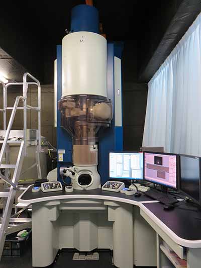
| Acc. Voltage | 200 kV, 80 kV, 60 kV with a Cold FEG and 2 Cs correctors (CL and OL) |
| Resolution | Point 0.11 nm / Lattice0.07 nm (TEM mode) 0.08nm (STEM mode) |
| Sample Tilting Angle | X / Y=±35° / ±30° |
| Observation/Analysis Functions | EELS analysis: GATAN Quantum (200 kV, 80 kV, 60 kV) EDS: Dual SDD Type (Detection surface area 2 × 100 mm2; Solid angle 1.96 sr=2 × 0.98 sr) Electron holography: Wave-front separation holography by use of an electron biprism Tomography |
| Images | 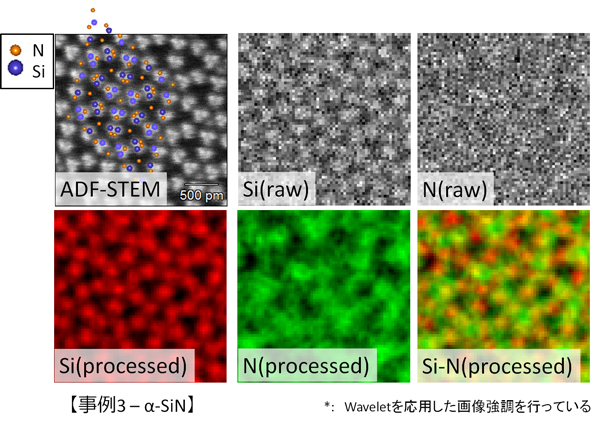 試料としてαタイプSiNを用いた。処理を施したNマップを見ると、強度は確かにNサイトで高くなっていることがわかる。一般にEDSは軽元素には不向きといわれているが、結晶性試料のようにチャネリングが利用できる場合原子分解能においても全く不可能でないことが分かる。 |