- Home
- > Research
- > Research Highlights
- > Vol. 36 Modulating Superconductivity ・・・
 Research Highlights
[Vol. 36]
Modulating Superconductivity of Two Dimensional Atomic Layers of Indium with Charge Transfer from Self-assembled Organic Molecules
- Previous
- Index
- Next
28 Mar, 2018
Charge and spin transfer from copper-phthalocyanine organic molecules self-assembled on superconducting atomic layers of indium modifies the superconducting transition temperature of the indium.

There have been tremendous advances in the self-assembly of organic molecules on solid surfaces via non-covalent bonds. Furthermore, research on self-assembly of two dimensional (2D) materials has yielded deep insights into the properties of superconducting 2D materials with atomic-scale thickness that could potentially lead to the creation of new hybrid materials and electronic devices through the so-called ‘bottom-up’ approach based on self-assembly as opposed to nanofabrication using etching and lithography. Notably, the unique physical proprieties of organic molecules offer advantages in terms of flexible and rational design and are an appealing approach with the possibility of opening up new fields of research.
With a view to controlling superconductivity in 2D atomic layers, Takashi Uchihashi and colleagues at International Center for Materials Nanoarchitectonics (WPI-MANA), National Institute for Materials Science,Tsukuba, Japan and collaborators at the Institute for Molecular Science, Okazaki, Japan, and Graduate School of Advanced Integration Science, Chiba University, Chiba, Japan, report the first observation of self-assembled organic molecules modulating the superconducting transport properties of an underlying 2D atomic-layer metallic material.
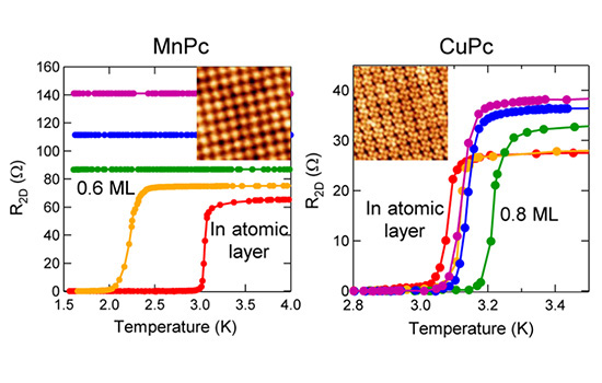
Specifically, the researchers fabricated 2D heterostructures consisting of an atomic layer of indium (In) epitaxially grown on a silicon substrate and a highly ordered metal-phthalocyanine (MPc, M = Mn, Cu) self-assembled onto the In layer. In this heterostructure, “charge transfer and local spins due to the presence of organic molecules modified the superconducting properties of the atomic layer”.
Examination of the 2D heterostructures led the researchers unexpectedly find that that substitution of the atom of metal-phthalocyanine from Mn to Cu changed the superconducting transition temperature (Tc) from 3.05 K to 3.20 K, that is, from a negative to positive direction. Further analysis combined with scanning tunneling microscopy (STM), X-ray magnetic circular dichroism (XMCD), and ab initio calculations revealed that this distinct phenomenon was due to competition between charge and spin effects.
“Particularly important is the directionality of the relevant d-orbitals that play a decisive role in magnetic interactions,” says Uchihashi. “It strongly suggests the feasibility of controlling macroscopic superconducting properties through manipulation of molecular states.”
Reference
“Controlled Modification of Superconductivity in Epitaxial Atomic Layer−Organic Molecule Heterostructures”
Shunsuke Yoshizawa[2], Emi Minamitani[3], Saranyan Vijayaraghavan[1], Puneet Mishra[1], Yasumasa Takagi[4], Toshihiko Yokoyama[4], Hiroaki Oba[5], Jun Nitta[5], Kazuyuki Sakamoto[5], Satoshi Watanabe[3], Tomonobu Nakayama[1], and Takashi Uchihashi[1]
Journal : Nano Lett. 17, 2287−2293, (2017).
DOI : 10.1021/acs.nanolett.6b05010
Affiliations
[1] International Center for Materials Nanoarchitectonics (WPI-MANA), National Institute for Materials Science, 1-1, Namiki, Tsukuba, Ibaraki 305-0044, Japan
[2] International Center for Young Scientists (ICYS), National Institute for Materials Science, 1-1, Namiki, Tsukuba, Ibaraki 305-0044, Japan
[3] Department of Materials Engineering, The University of Tokyo, 7-3-1, Hongo, Bunkyo-ku, Tokyo 113-8656, Japan
[4] Institute for Molecular Science, Myoudaiji Campus, 38 Nishigo-Naka, Myodaiji, Okazaki, Aichi 444-8585, Japan
[5] Department of Nanomaterials Science, Graduate School of Advanced Integration Science, Chiba University, 1-33 Yayoi-cho, Inage-ku, Chiba 263-8522, Japan
Contact information
Research Center for Materials Nanoarchitectonics (MANA)
National Institute for Materials Science
1-1 Namiki, Tsukuba, Ibaraki 305-0044 Japan
Phone: +81-29-860-4710
E-mail: mana-pr[AT]nims.go.jp
1-1 Namiki, Tsukuba, Ibaraki 305-0044 Japan
Phone: +81-29-860-4710
E-mail: mana-pr[AT]nims.go.jp