 Press Release 2011
World Highest Performance Nanodielectrics
Simple and direct, the proposed method provides remarkable spatial and temporal insights into the dynamics of resistive hot-spots and millisecond-paced thermal variations occurring inside nanoscaled carbon nanotubular interconnects.
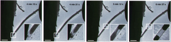
Figure 1. Dynamics of hot spot migration along a Joule-heated sulfide-filled carbon nanotube connected to two gold electrodes in a transmission electron microscope.
From left to right: Consecutive TEM images (the running time is shown) illustrating the movement of the hot spot from the contact point on the left towards the more central part of the tube. The insets show the enlarged boxed areas. Each segment front acts as a marker for the sulfide sublimation temperature (928 K). Plus and minus signs mark the areas where the current temperature is respectively higher and lower than the sulfide sublimation temperature. Scale bar, 0.5 µm.
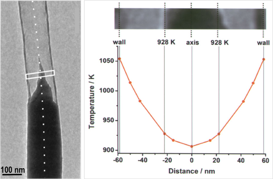
Figure 2. Estimate of the radial temperature profile in an electrically-heated CNT channel.
Left panel: Section of a partially empty CNT filled with a sublimable Zn0.92Ga0.08S compound showing a sharp conical needle. The dotted line marks the nanotube main axis. The box encloses the area where the temperature profile was estimated from.
Right panel: Plot of the temperature variation across the nanotube´s channel. The image at the top corresponds to the box in the left panel. The sublimation temperature of the sulfide is coincident with the surface layers of the conical needle.
Further information
Affiliations
- 1.International Center for Materials Nanoarchitectonics (WPI-MANA), National Institute for Materials Science (NIMS)
- 2.University of Aveiro, Portugal
- 3.JNCASR, Bangalore, India