 Press Release 2011
Success in Clarifying Behavior of Impurities in Silicon Nanowire with Diameter of 1/50,000mm
-Toward Realization of Next-Generation Type Transistors and Nanowire Photovoltaic Cell Materials-
A research group led by Dr. Naoki Fukata and a group under Prof. Koichi Murakami of the University of Tsukuba succeeded in non-destructive, non-contact detection of the states of impurities introduced as dopants for carrier control in silicon nanowires (diameter: <20nm). The research groups also succeeded in clarifying the behavior of those impurities.
This work is a step toward the realization of next-generation transistors. The assessment method is also considered a promising approach for assessment of photovoltaic cells.
This work is a step toward the realization of next-generation transistors. The assessment method is also considered a promising approach for assessment of photovoltaic cells.

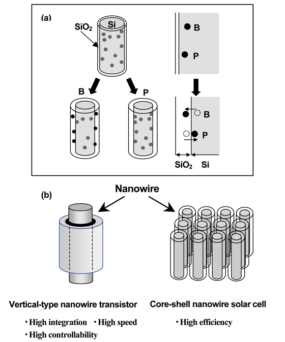
Figure 1. Schematic of (a) segregation behavios of dopant atoms in Si nanowires and (b) application to the next-generation vertical-type nanowire-transistor and core-shell nanowire solar cells.
Further information
Affiliations
Naoki Fukata1, 2, Shinya Ishida3, Shigeki Yokono3, Ryo Takiguchi3, Jun Chen4, Takashi Sekiguchi4, Kouichi Murakami3
- 1.International Center for Materials Nanoarchitectonics (WPI-MANA), National Institute for Materials Science (NIMS)
- 2.PRESTO, Japan Science and Technology Agency
- 3.Institute of Applied Physics, University of Tsukuba
- 4.Advanced Electronic Materials Center, National Institute for Materials Science

