 News 2012
Summer Science Camp 2012 was successfuly held
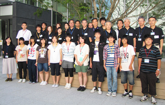
Group photo of the participants and instructors.
Observation of the nano-scale world
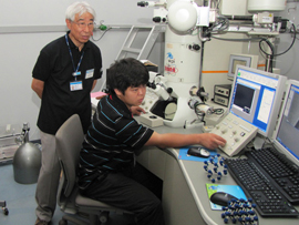
Fine structure observation by Scanning Electronic Microscope (SEM)
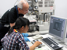
A participant operates SEM.
Taking a SEM image of butterfly scales.
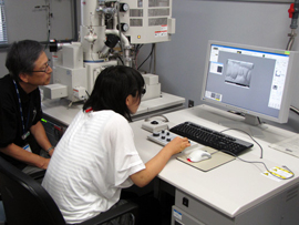
Atomic scale observation by Transmission Electron Microscope (TEM)
Explanation about EDX measurement.
A participant operates TEM to take a photo image of a crystal lattice.
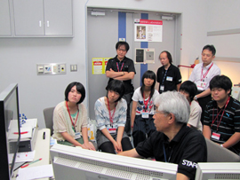
Working inside the clean room
Learning lithography
Inside the clean room, the participants experienced two kinds of photolithography including a “positive-type process” and a “negative-type process” to learn about semiconductor manufacturing. To observe the difference between the two types of processes, the participants checked and compared the results under the microscope.
Then they used photolithography to make two types of Au-electrode wires with and without dust to verify the sensitivity to environmental contamination. By I-V measurements and SEM observation of the electrode structure, the participants learned that even a single nano-scale dust can cause short-circuit in an electrode, which is the reason why semiconductor processing needs an environment with a controlled level of contamination.
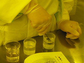
Carefully rinsing a chip with water.
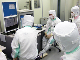
Verifying the sensitivity of an electrode to
contamination.
Presentinon of the results
Presentation by group A.
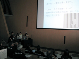
Presentation by group B.
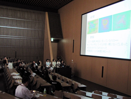
Other lecture and a reception
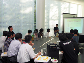
A lecture by Dr. Yoshio Bando.
A young researcher answers to a question of a participant.