
Group
界面機能グループ Functional Heterointerfaces Group
Result H23
界面制御による光・電子機能デバイスの開拓
Exploration of Optical and Electronic Functional Devices with Control of Interfaces
K. Sakamoto, J. Ueno, K. Bulgarevich, and K. Miki, Appl. Phys. Lett. 2012, 100, 123301.
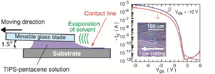
高性能有機デバイスの開発: 改良されたフロー・コーティング法により高配向TIPS-ペンタセン層を形成し、ボトムゲート・ボトムコンタクト型有機トランジスタを作製した。フロー・コーティング方向にTIPS-ペンタセン結晶のa軸が配向した。フロー・コーティング方向にチャネル電流を流したときの電界効果移動度は0.87 cm2V-1s-1であった。
To realize high performance organic devices, we are developing alignment control techniques applicable to wet device fabrication processes. Using a modified flow-coating method, we succeeded in fabricating highly oriented TIPS-pentacene organic field-effect transistors with a bottom gate/bottom contact structure. We found that the crystallographic a-axis is highly aligned parallel or antiparallel to the flow-coating direction. The field-effect mobility along the flow-coating direction was 0.87 cm2V-1s-1.
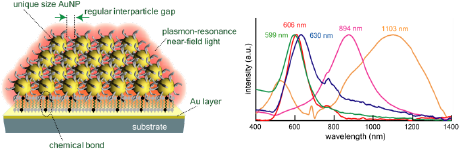
近接場光源の大面積化: 近接場光は回折限界を超える分解能を可能とし、50nm程度の分解能を持つ近接場光顕微鏡の原理となったナノテクノロジーの一つである。光としての近接場光は量子物理、化学、通信など広く応用されているが、光センサー、太陽電池、光化学反応などへの実用化には平方cmから平方m程度の大面積の光源が必要になる。その為、ナノスケールの金ナノ粒子表面で発生する近接場光を配列化することにより、金ナノ粒子配列全面で近接場光を発生させて大面積化を行った。
Large-area near-field light source: Use in various technologies such as optical sensors, photovoltaic cells is needs “near-field light” sources on a substrate with a size of 1cm2or more. We developed light sources is a large-area light source in which near-field light is generated over the entire surface of the Au nanoparticle array by forming an array of the near-field light sources generated at the Au nanoparticles.
特許出願 PCT/JP2011/054963-5 (2011.3.3)他