
Group
界面機能グループ Functional Heterointerfaces Group
Result H22
高性能・高機能有機デバイスの開発
Development of high performance and high functional organic devices
[1] K. Sakamoto, K. Miki, M. Misaki, K. Sakaguchi, Y. Hijikata, M. Chikamatsu, and R. Azumi, J. Appl. Phys. 107, 113108 (2010).
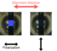
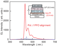
ポリイミド光配向膜を用いることによって、青色発光高分子材料として注目されているポリフルオレン(PFO)を高い配向秩序度で配向させることができます。我々は、極薄ポリイミド光配向膜を高分子電界発光(EL)素子構造に挿入することによって、偏光高分子EL素子を作製することができます。光配向膜の厚さ、PFO発光層の厚さを最適化することによって、偏光比46 (波長434 nm)、電流効率0.3 cd/A (150 cd/m2)の偏光EL素子を作製することに成功しました。[1]
Polyfluorene (PFO), which is a promissing blue light-emitting polyer, can be aligned by photo-aligned polyimide (PI) film as the alignment layer. Polymer-based light-emittind diodes (PLEDs) can be fabricated by inserting a very thin photo-aligned PI layer into the device structure. By optimizing thickness of the photo-aligned PI film and th PFO light-emitting layer, we succeeded in fabricating a PLED showing a polarization ratio 46 at 434 nm and a current efficiency of 0.3 cd/A at 150 cd/m2. [1]
大面積近接場光源としての金ナノ粒子2次元配列
Chemical coating of large-area Au nanoparticle two-dimensional arrays as plasmon-resonant optics
[2] K. Isozaki, T. Ochiai, T. Taguchi, K. Nittoh, and K. Miki, Appl. Phys. Lett. 97, 221101. (2010)
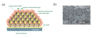
電気泳動と気-液界面における自己組織化、化学結合による固定化を組み合わせたハイブリッド型の金ナノ粒子2次元配列作製法を開発しました。[2]大面積 基板上に高被覆率(>95%)で局在表面プラズモンを発生する金ナノ粒子を配列固定化できるため、大面積近接場光源としての応用が期待されていま す。
We have developed a hybrid fabrication method for gold nanoparticle two-dimensional arrays by applying electrophoresis, self-organization at gas-liquid interface, and immobilization with chemical bonds together. [2] This method enables us to fabricate large-area gold nanoparticle two-dimensional arrays with high coverage and mechanical strength. We expect this substrate leads to the broad application as a large-area near-field light source.