
Group
界面機能グループ Functional Heterointerfaces Group
Research
高性能・高機能有機デバイスの開発
Development of high performance and high functional organic devices
高性能・高機能の有機デバイスを実現するために、デバイス作製工程に適用可能な有機分子の配向制御技術を開発しています。分子配向を制御して発光層を形成することによって偏光発光素子を作製できます。また、有機トランジスタの活性層の分子配向を制御することにより、高移動度有機トランジスタの実現、素子特性のバラツキの低減が期待されています。
To realize high performance and high functional organic devices, we are developing alignment control methods applicable for organic device fabrication processes. By aligning light-emitting molecules, polarized light-emitting diodes can be fabricated. By aligning the organic semiconductor molecules, organic field-effect transistors with high charge carrier mobility can be realized. In addition to this, if the molecular orientation can be controlled for each device, the device-to-device variation of the electric properties is expected to be minimized.
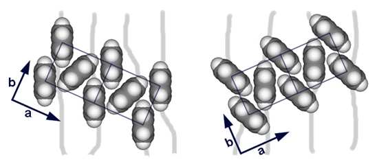
Alignment control of pentacene molecules by photo-aligned polyimide films. [Phys. Rev. Lett. 101. 236103 (2008).]
近接場リアクターに関する研究
Development of near-field photochemical reactors
金属ナノ粒子の局在表面プラズモンを励起源とした近接場光反応によってエネルギー効率の高い光化学プロセスの開発を目指します。数ナノメートル間隔で配列された金属ナノ粒子の間隙では局在表面プラズモンの共鳴に基づく増強電磁場による多光子過程を利用することもできます。マイクロリアクター内部に金属ナノ粒子を配列固定化することで、ナノメートルスケールの極微小領域に局在化する高強度の光を効率良く励起源とした光化学反応が可能となります。
We develop highly efficient photochemical processes by means of near-field photochemical reactions using localized surface plasmon of metallic nanoparticles as a nano-scale light source. Multi-photon processes are also available at the gap of closely-arrayed metallic nanoparticles with nanometers intervals. Near-field photochemical reactor, containing inside-immobilized metallic nanoparticle arrays, are expected to demonstrate highly efficient photochemical processes based on the enhanced electromagnetic field.
