Real Working Environmental Electron Holography Microscope
JEM-ARM200F-B (JEOL)
Sengen-site, Fine Processing Lab. #125This microscope has TEM image and STEM probe aberration correctors for high-resolution observations. Cold FEG enables high-resolution STEM even at low acceleration voltage. EELS and energy filter image acquisition is possible.
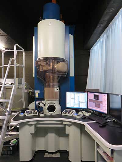
| Acc. Voltage | 200 kV, 80 kV, 60 kV with a Cold FEG and 2 Cs correctors (CL and OL) |
| Resolution | Point 0.11 nm / Lattice0.07 nm (TEM mode) 0.08nm (STEM mode) |
| Sample Tilting Angle | X / Y=±35° / ±30° |
| Observation/Analysis Functions | EELS analysis: GATAN Quantum (200 kV, 80 kV, 60 kV) EDS: Dual SDD Type (Detection surface area 2 × 100 mm2; Solid angle 1.96 sr=2 × 0.98 sr) Electron holography: Wave-front separation holography by use of an electron biprism Tomography |
| Images | 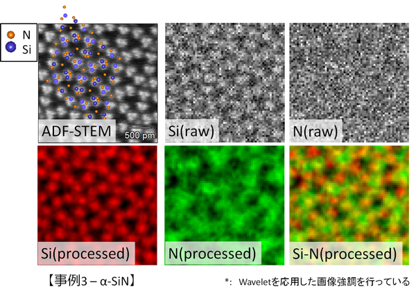 The specimen used is an a-type SiN. You can see from the processed N map, that the strength is certainly stronger on the N site. Typically, it is said that EDS is not suited for light elements, but if channeling can be used as in the case of crystalline samples, EDS analysis is not impossible even for atomic resolutions. |