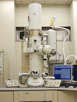
200kV Field Emission Transmission Electron Microscope
JEM-2100F1 (JEOL)
Sengen-site, Physical Analysis Lab. #126The microscope has a user-friendly operation interface. It supports the following modes: TEM, STEM, EELS、EDS,NBD and CBED. It is also equipped with a CCD camera for diffraction pattern. Three-dimensional observation is possible with a dedicated holder and tomography software.
| Electron Gun | Schottky field emission gun |
| Acc. Voltage | 200kV, 100kV, 120kV |
| Resolution | Point: 0.23 nm, Lattice: 0.10 nm (TEM mode) 0.2 nm (STEM mode) |
| Spherical / Chromatic Aberration | 1.0mm / 1.4mm |
| Sample Tilting Angle | X : ±35°, Y : ±30° |
| Spot Size | 0.5 nm (smallest)for NBD, CBD & EDS |
| Observation/Analysis Functions | STEM: ADF and BF EDS: Spot analysis and Elemental mapping EELS analysis: GATAN Enfina CCD Camera 1: Maximum Pixel Size 4008 × 2672 CCD Camera 2: for Diffraction Pattern, Maximum Pixel Size 2048 × 2048 Tomography Special specimen holder: Heating specimen holder; Cooling specimen holder, Tomography specimen holder |
| Images | 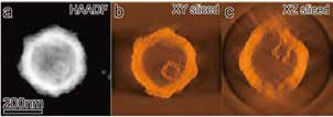 TEM-CT observation of mesoporous silica shells. |