Facilities
Research Laboratory Equipment
For a comprehensive list of equipment, please visit the Facilities in 2D Quantum Materials Group.
Key Research Instruments
- Continuous-wave (CW) tunable Ti:sapphire laser system (690–950 nm wavelength range)
- Multiple laser sources including He-Ne and solid-state lasers (1550 nm, 1310 nm, 532 nm, and 304 nm)
- High-sensitivity visible CCD detector and precision spectrometer
- Advanced helium flow cryostat for low-temperature measurements
- High-precision microscopes with automated motorized stages
- State-of-the-art photochemical reactor
Advanced Characterization Capabilities
- Photoluminescence spectroscopy for optical property analysis
- Time-resolved photoluminescence for carrier dynamics studies
- Photon correlation measurements using Hanbury Brown-Twiss (HBT) interferometry
- Differential reflection spectroscopy for material characterization
- Raman spectroscopy for structural analysis
- Photocurrent spectroscopy with spatial mapping capabilities
Shared Research Facilities
NIMS Nanofabrication Facility
Our research group has access to NIMS’s state-of-the-art microfabrication cleanroom, enabling the fabrication of advanced nanoscale electronic devices.
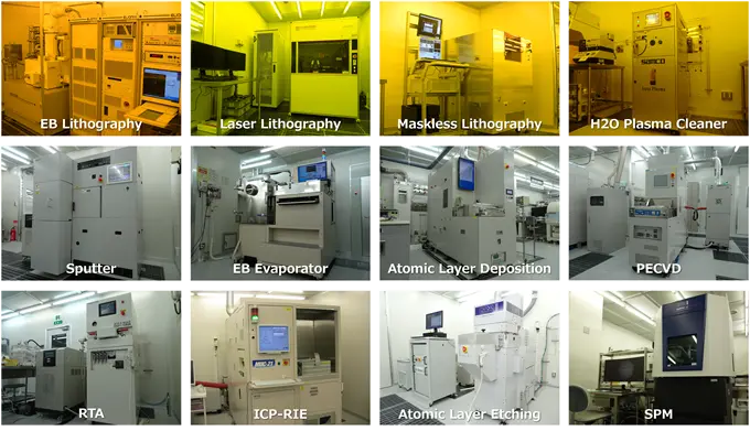
The facility offers comprehensive nanofabrication capabilities:
- Advanced Lithography: High-precision patterning through electron beam and photolithography techniques
- Thin Film Deposition: State-of-the-art thin film growth via sputtering, chemical vapor deposition (CVD), and atomic layer deposition (ALD)
- Precision Etching: Advanced material processing using reactive ion etching (RIE) and ion milling
- Characterization Tools: High-resolution imaging and metrology systems for nanoscale structure analysis