Japanese page is here.
Japanese page is here.
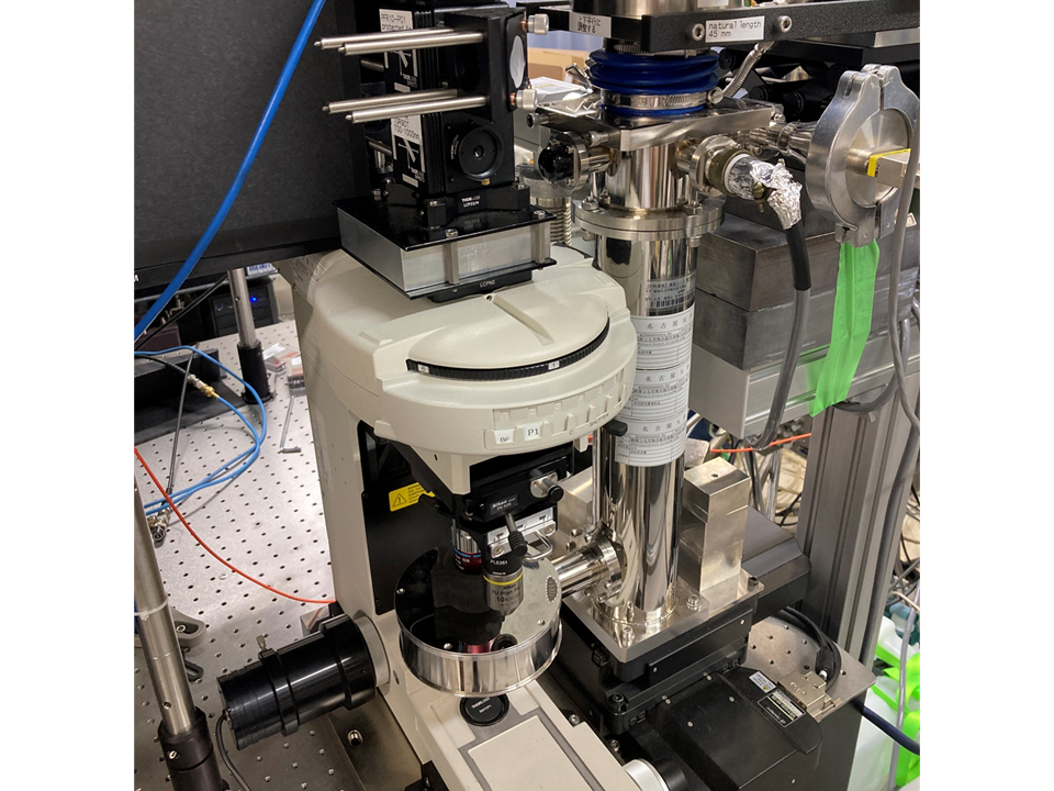
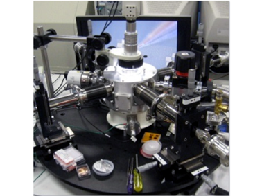
Home-built microspectroscopy system (an upright microscope with a vertical objective lens and an ARS cryostat). Various spectroscopic measurements at cryogenic temperatures are possible.
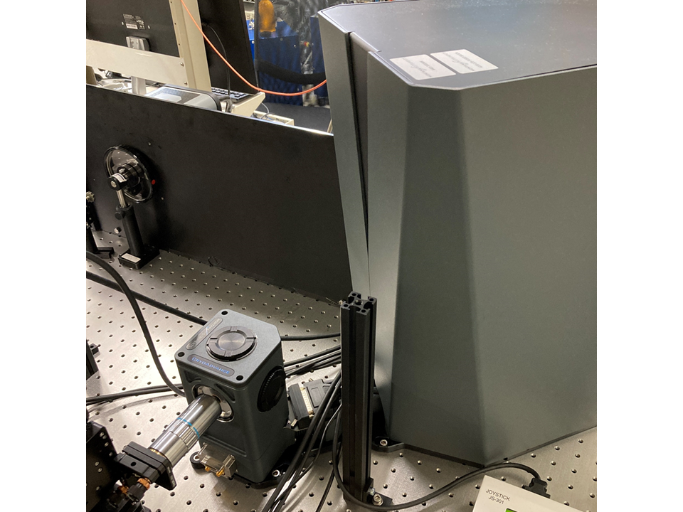
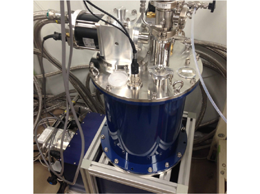
Microspectroscopy system (a Montana Ins cryostat and a nanopositioner). A variety of applications, including spectroscopic measurements using ultrashort pulsed laser at 3.5 K, can be performed.
Optical system for converting the white light emitted from the supercontinuum light into a parallel beam of desired wavelength (500-2000 nm). A HeNe laser and various semiconductor lasers are also available.
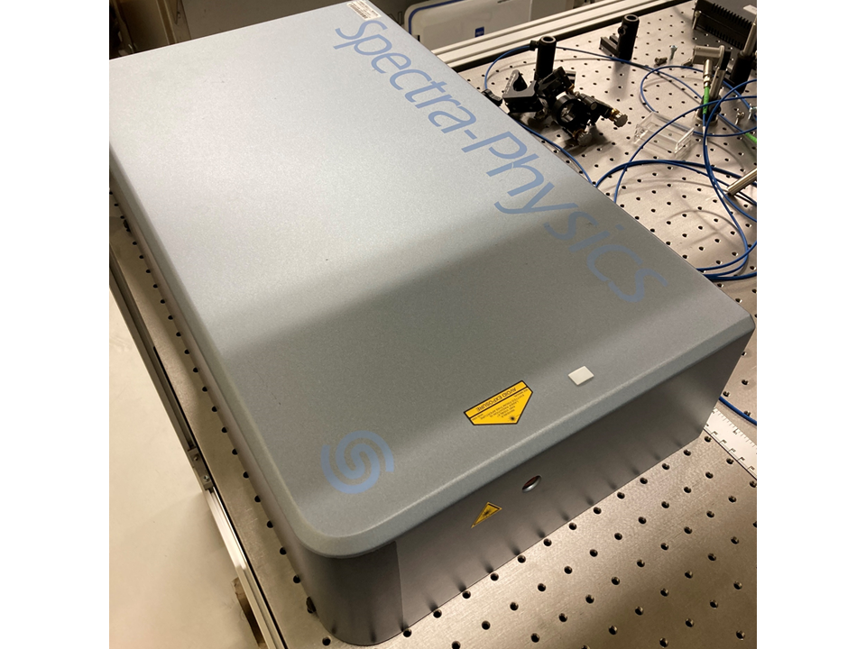
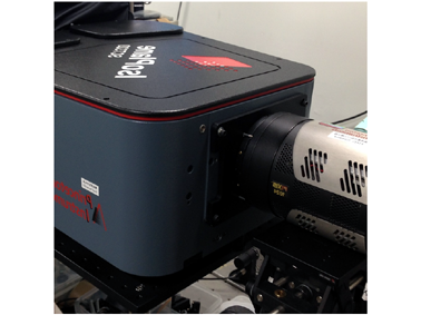
One-box Ti:sapphire ultrashort pulsed laser (Mai Tai HP). In addition to various time-resolved measurements, it can be used to determine crystal orientation by observing second harmonic generation.
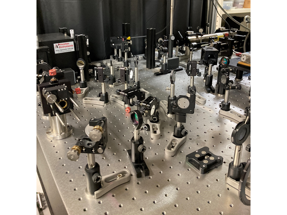
Aberration-free spectrometer used for microspectroscopy (two IsoPlane 320 and one HRS-300). Used in combination with liquid-nitrogen-cooled CCD, thermoelectrically-cooled CCD, and EMCCD.
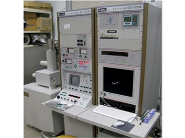
This system is used to measure FET properties of devices fabricated. Measurements down to 10 K is possible.
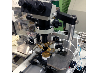
A simple probe station to check device properties at room temperature
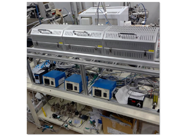
Transport measurements at 4 〜 300 K and 0 〜 6 Tesla are possible.
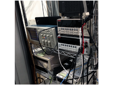
For electrical measurements: nanovoltmeters, AC/DC current sources, electrometers, multimeters, lock-in amplifiers
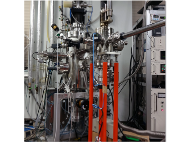
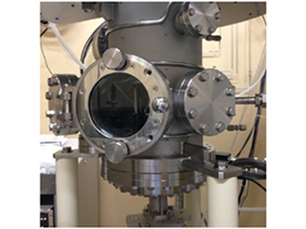
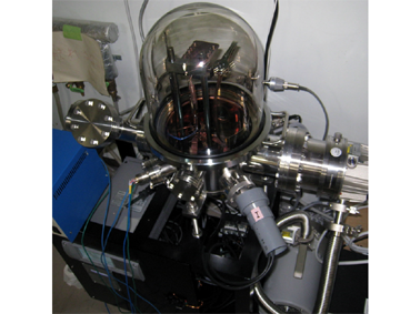
MBE growth of various 2D materials are possible. E-beam heating, K-cells, evaporators are used to supply various sources.
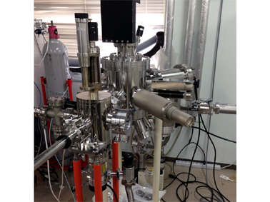
In addition to evaporators and K-cells, RHEED is available to monitor crystal growth.
A cold-wall MOCVD chamber for crystal growth of 2D materials. Sources are supplied from top of the chamber as vapor, and the source supply can be controlled automatically by a valve on/off system.
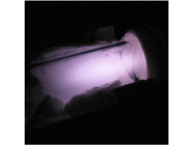
A three-furnace CVD chamber for crystal growth of TMD-based 2D materials
Fine patterns can be fabricated with focused electron beam. This is an indispensable setup for device fabrications.
Home-built vacuum deposition system. This is used for deposition of electrodes.
Home-built plasma clearner for removal of amorphous carbon impurities
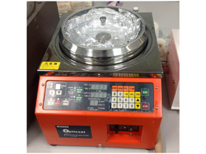
This spin coater is mainly used to coat a resist layer for the lithography process.
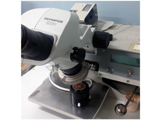
This is used to make electrical contacts to devices fabricated.
