Some examples of 3DAP analysis by NIMS are shown in this page.
Grain boundary in Dy-diffusion processed Nd-Fe-B sintered magnet
The 3D atom map shows the distributions of Nd, Ga, and Cu atoms. A grain boundary can be clearly visible from the difference in the orientation of the lattice planes. The grain boundary is enriched with Nd, Ga and Cu. Both Cu and Ga are segregated at the interfaces between the Nd-rich grain boundary phase and the Nd2Fe14B grains.
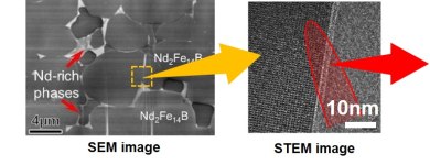
SEM image of Nd-Fe-B magnet (left)
STEM image of grain boundary (right)
STEM image of grain boundary (right)
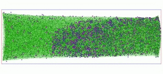
(● Nd ● Ga ● Cu)
3D atom map of Nd-enriched grain boundary phase in a Dy-diffusion processed Nd-Fe-B sintered magnet ~35×35×110 nm3
3D atom map of Nd-enriched grain boundary phase in a Dy-diffusion processed Nd-Fe-B sintered magnet ~35×35×110 nm3
Bake-hardenable Mg–Al–Zn–Mn–Ca sheet alloy
Characterization of microstructure of Mg–Al–Zn–Mn–Ca sheet alloy using the correlative TEM-APT technique are shown below.
Two-beam BF-TEM image (left), Correlative 3D atom map from the tip of the same sample shown in TEM image (center), Overlay of 3D atom map and the corresponding region in TEM image (right)
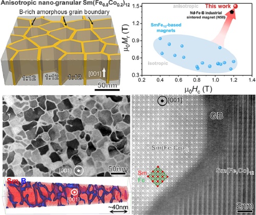
Boron doped Sm(Fe0.8Co0.2)12 anisotropic magnetic thin film
NIMS and Tohoku Gakuin University have developed a boron-doped anisotropic Sm(Fe0.8Co0.2)12 thin film containing only small amount of rare earth elements. The compound exhibited 1.2 tesla coercivity, sufficient for use in automotive electric motors. This was achieved by creating a unique granular nanostructure in which Sm(Fe0.8Co0.2)12 grains are uniformly enveloped by an amorphous grain boundary phase approximately 3 nm in thickness. This compound exhibited superior magnetic properties to that of Nd-Fe-B based magnets even when processed into a thin film.
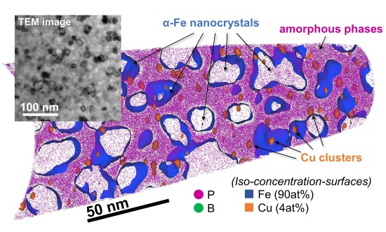
Nanocrystalline soft magnetic materials
Nanocrystalline soft magnetic materials were investigated using Transmission Electron Microscopy and Atom Probe Tomography.
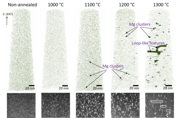
Implanted Mg in annealed GaN layers on free-standing GaN substrates
3D atom maps of Mg and LAADF-STEM images for non-annealed and 1000C, 1100C, 1200C, and 1300C annealed Mg implanted GaN samples are shown below. Implanted Mg concentration is 1x1019cm-3(~0.01at.%) for all samples.
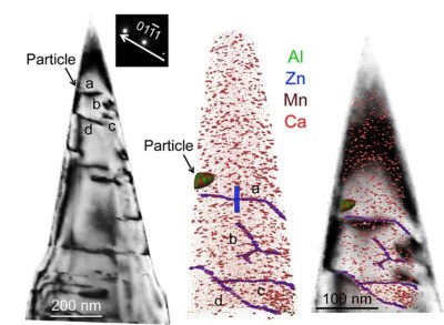
Bulk insulator ceramics - ZrO2-MgAl2O4
NIMS has developed an original laser atom probe and was the first in the world to succeed in atom probe analysis of bulk insulators using an ultraviolet laser.
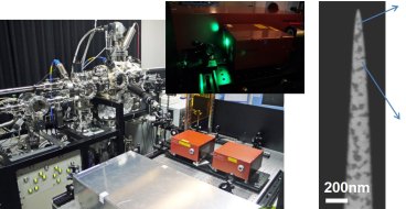
Laser assisted 3DAP developed by NIMS (left)
SEM image of tip for 3DAP measurement (right)
SEM image of tip for 3DAP measurement (right)
(● Mg ● Al)
3D atom map ~65×65×270 nm3
3D atom map ~65×65×270 nm3
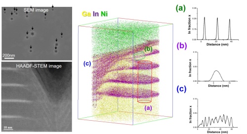
GaInN/GaN multiple quantum wells in V-shaped pits
The 3DAP method can precisely analyze the distribution of elements within a nanoscale device or the uneven distribution of nanoscale elements within a material.
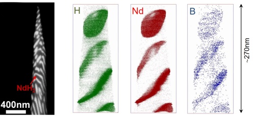
Hydrogenation-disproportionated Nd-Fe-B powders
The 3DAP method can detect and identify the position of single atoms including light elements like Hydrogen, which are difficult to observe with electron microscopes.
GaN nanowires and GaInN/GaN multi-quantum shells
The development of the microfabrication method using the focused ion beam (FIB) technique makes site specific 3DAP specimen preparation possible, such as grain boundaries, interphase interfaces, specific region of devices.
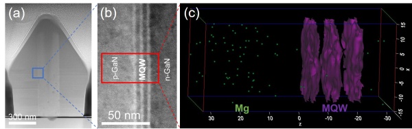
(a) HAADF-STEM image of GaN nanowire, (b) Magnified HAADF-STEM image of MQW, (c) 3D atom map from MQW and p-GaN region.
Nanoscale voids in Sb-doped p-type ZnO nanowires
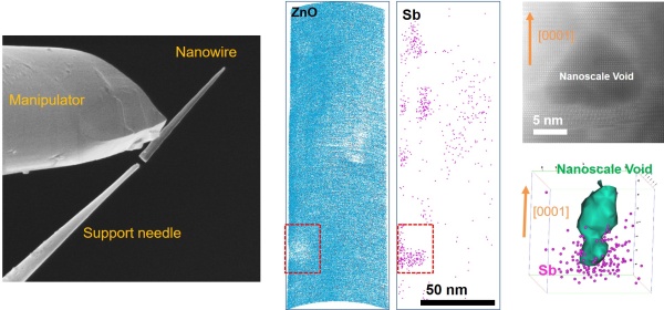
Preparation of 3DAP specimen (left)
Sliced 3D atom maps (center)
HAADF-STEM image of nanoscale void in the nanowires (right top)
Sliced 3D atom maps (center)
HAADF-STEM image of nanoscale void in the nanowires (right top)
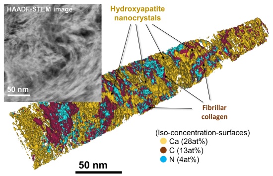
Pig tooth dentin