 Press Release 2021
Development of Ultra-High-Resolution Printed Electronics Using Dual Surface Architectonics
C-INK Co., Ltd.
Priways Co., Ltd.
NIMS has developed a dual surface architectonic process which enables to print submicrometer-scale circuit patterns by increasing the chemical polarity of predetermined areas on surface, thereby promoting selective adhesion of metallic nanoparticles to these areas.
“Dual Surface Architectonics for Directed Self-Assembly of Ultrahigh-resolution Electronics”
Lingying Li, Wanli Li, Qingqing Sun, Xuying Liu, Jinting Jiu, Mizuki Tenjimbayashi, Masayuki Kanehara, Tomonobu Nakayama, and Takeo Minari ;
Journal: Small [May 14, 2021];
DOI : 10.1002/smll.202101754)
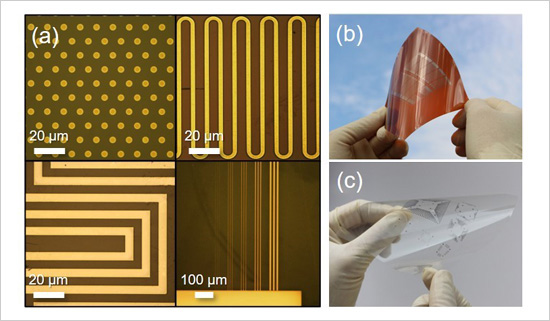
Figure. (a) Microcircuit patterns printed using a dual surface architectonic process. Circuits printed on polyimide (b) and transparent (c) films.
Abstract
Printed electronics—electronic circuits printed using metallic and semiconducting inks—have been developed for a wide range of applications. However, the circuit traces printable using existing printing technologies, such as inkjet and screen printing, are too wide for certain applications. New technologies capable of printing finer circuit traces therefore had to be developed.
This research team recently developed a dual surface architectonic process which can be used to print submicrometer-scale wiring patterns by increasing the chemical polarity of predetermined microscopic areas of a substrate surface, thereby promoting selective adhesion of metallic nanoparticles to these areas. Simple photo and chemical treatments are applied to the substrate during this process. First, preselected surface areas are activated by ultraviolet irradiation. A chemical treatment is then applied to these areas which increases chemical polarity and surface energy only in the UV-activated surface areas. Consequently, the surface’s adhesiveness to metallic ink increases precisely in the treated areas. Because both treatments are simple and quick and can be performed in ambient air, use of the dual surface architectonic process is expected to significantly expedite and reduce the cost of printable electronic manufacturing processes compared to photolithography and other conventional printing methods.
Priways Co., Ltd. and C-INK Co., Ltd. have developed a metallic nanoparticle self-assembly system which can be used to print metallic nanoparticle inks at ultra-high resolution. The system will soon be put on sale along with primers specifically designed for use with it to enhance adhesion of metallic inks to different types of substrates. This research team will promote widespread use of this ultra-high-resolution printing technology for the production of printed electronics.
This project was carried out by a research team led by Takeo Minari (Leader of the Printed Electronics Group, Research Center for Functional Materials (RCFM), NIMS), Tomonobu Nakayama (Deputy Director of the International Center for Materials Nanoarchitectonics (MANA), NIMS), Lingying Li (a recipient of the JSPS Research Fellowship for Young Scientists, MANA, NIMS), Mizuki Tenjimbayashi (Independent Scientist, MANA, NIMS), Masayuki Kanehara (CEO, C-INK Co., Ltd.) and Hayato Kawashima (CEO, Priways Co., Ltd.). This work was conducted in conjunction with three other projects: 1) three-dimensional flexible circuit R&D at the NIMS Center for Functional Sensors & Actuators, 2) a Tsukuba Innovation Ecosystem project to commercialize systems capable of printing metallic ink microcircuit patterns and 3) a project entitled “Submicron-scale selective metallization process for 3D integration technology” funded by the JSPS Grant-in-Aid for Scientific Research (B).
This research was published in the online version of Small, a German scientific journal, on May 14, 2021.
(Regarding this research)
Takeo Minari
Group Leader
Printed Electronics Group
Research Center for Functional Materials
National Institute for Materials Science
Tel:+81-29-860-4918
E-Mail:MINARI.Takeo=nims.go.jp
(Please change "=" to "@")
Masayuki Kanehara
CEO, C-INK Co., Ltd.
E-Mail:info=cink.co.jp
(Please change "=" to "@")
Hayato Kawashima
CEO, Priways Co., Ltd.
E-Mail:info=priways.co.jp
(Please change "=" to "@")
(General information)
Public Relations Office
National Institute for Materials Science
Tel:+81-29-859-2026
Fax:+81-29-859-2017
E-Mail:pressrelease=ml.nims.go.jp
(Please change "=" to "@")