 Press Release 2014
In the demonstration project for practical application at the Kanagawa Academy of Science and Technology (KAST), the research group led by Dr. Tetsuya Hasegawa (Professor, University of Tokyo; KAST principal researcher), Dr. Yasushi Hirose (Research Associate, University of Tokyo; KAST researcher) and Mr. Kenji Taira (postgraduate student, University of Tokyo; KAST research assistant), in collaboration with the team led by Dr. Takayoshi Sasaki (NIMS Fellow), developed a method for growing high-quality oxide thin films on a glass substrate which is an affordable material.
Solid phase crystallization (SPC) is a technique for crystallizing amorphous thin films of a target substance on a substrate by heat treatment and thereby obtaining thin film crystals consisting of large crystal grains, and it is known as a method for growing thin film crystals consisting of large crystal grains of a few to a few dozen micrometers. However, as this method is incapable of controlling the orientation of crystal grains on a substrate made of affordable materials, such as glass or plastic, it was impossible to fabricate thin films with adequate performance from highly anisotropic substances by this method.
The research group succeeded in growing thin film crystals consisting of highly oriented crystal grains, which were as large as a few micrometers or more, by coating a glass substrate with oxide sheets of about one nanometer in thickness, called oxide nanosheets, and using these nanocrystals as seed crystals in SPC. The method employed in this research was an upgraded version of the nanosheet seed layer method published by NIMS in 2009 (see Reference 1). In the nanosheet seed layer method, a glass substrate is covered with oxide nanosheets, which are delaminated two-dimensional oxide crystals of about 1nm in thickness, and used just like a pseudo single-crystal substrate. Although this method is superior in obtaining highly oriented thin film crystals, it has a disadvantage in that the size of the resulting crystal grains cannot be larger than the size of the oxide nanosheet (generally a few micrometers or smaller). By combining the nanosheet seed layer method with SPC, the research group at KAST succeeded in growing crystal grains in the lateral direction to a size of more than a few micrometers. The titanium oxide transparent conductive films fabricated on the glass substrate by this new method exhibited low electrical resistance (3.6×10⁻⁴Ωcm) and mobility (13cm2V-1s-1), comparable to thin films grown on a single-crystal substrate.
The new method has been confirmed to also be applicable to strontium titanate, a typical substance used in electronics, and thus it is expected to promote the development of low-cost and high-performance devices using oxide thin film crystals.

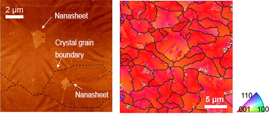
(left) An atomic force microscope image of the titanium oxide thin film fabricated by the new method, showing that nanosheets, which provided seed crystals, exist at the center of crystal grains.
(right) A map of crystal grain orientation determined by electron backscattering diffraction. The black lines correspond to the boundaries of individual crystal grains and the color represents their orientation. All crystal grains are highly (001) oriented.
For more detail about research
The University of Tokyo, Department of Chemistry
Prof. Tetsuya Hasegawa
Tel:+81-3-5841-4353
E-Mail:hasegawa=chem.s.u-tokyo.ac.jp
(Please change "=" to "@")
 Press Release 2014

