Laser-Assisted Atom Probe Tomography
In conventional atom probe tomography (APT) before the early 2000s, atoms at the tip apex were field evaporated by applying nanosecond (ns) high-voltage pulses superimposed on a DC standing voltage. This required specimens to be electrically conductive, making metals the primary application area for the APT technique. Although some studies reported the analysis of highly doped silicon (10-2 Ohm·cm) and thin oxide film layers, it was generally believed that materials with higher electrical resistivity could not be analyzed. To overcome this fundamental limitation of APT, laser-assisted field evaporation was proposed. Attempts at laser-assisted field evaporation were made in the 1970s by various APT groups; however, due to the limited performance of laser systems at that time, laser-assisted APT was largely abandoned. In 2004, the APT group at Université de Rouen Normandie revived laser-assisted APT by employing femtosecond (fs) pulsed lasers in their tomographic atom probe (TAP). Since then, several APT groups have implemented either picosecond (ps) or femtosecond (fs) lasers in APT, and it is now well established that laser-assisted field evaporation has greatly expanded the application areas of APT to include metals, semiconductors and their devices, and even highly insulating materials.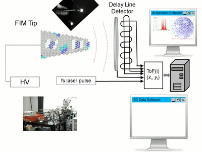
Fig. 1. Schematic illustration (GIF animation) of laser-assisted atom probe tomography (APT).
As shown in Fig. 1, laser-assisted APT operates in the same manner as voltage-pulsed APT, except that atoms are field evaporated by irradiation with laser pulses. Several studies have demonstrated that employing shorter wavelength laser pulses can substantially improve mass resolution. This suggests that the field evaporation mechanism is not purely thermal when short wavelength lasers are used. With improved mass resolution, it is possible to reduce the flight distance and thus maintain a large acceptance angle. NIMS has also discovered that the use of short-wavelength lasers (UV: 355 nm) enables field evaporation of insulating ceramics, allowing even bulk insulator ceramics to be analyzed using laser-assisted APT (Y.M. Chen et al., Scripta Materialia 61, 693-696 (2009)).
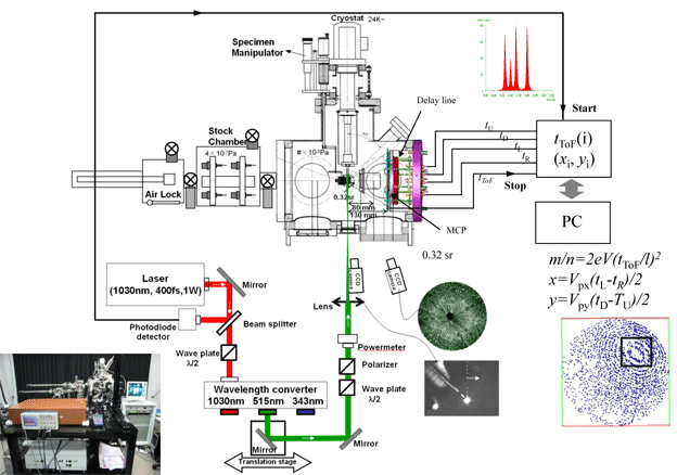
Fig. 2. Schematic illustration of the laser-assisted wide angle APT developed by NIMS.
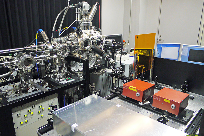
Fig. 3. Photo of fs-laser-assisted APT developed by NIMS.