Crystal structure analysis using advanced STEM
The characterization of nano-structure that realizes materials' properties is an ultimate objective of electron microscopy. Scanning transmission electron microscopy (STEM) is an effective tool for microstructure analysis. Annular dark-field (ADF) imaging in STEM has several advantages such as compositional sensitivity and intuitive interpretability. Our purpose of this study is to develop the local crystal analysis based on the STEM.
Development of dedicated STEM instrument with high stability
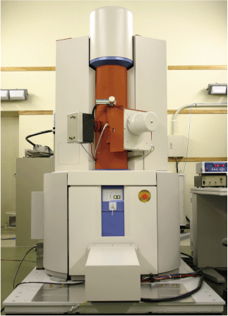
We developed a dedicated scanning transmission electron microscope with high stability. The mechanical and electronic stabilities of the microscope were substantially improved, e.g. the specimen drift rate was found to be less than 0.2 nm/min. The stabilized STEM instrument allows us to acquire distortion-free STEM images and high-signal to noise ratio analyses.
K. Kimoto et al. J. Electron Micrsc., 56 (2007) 17.
Software technique to realize inherent performance of STEM
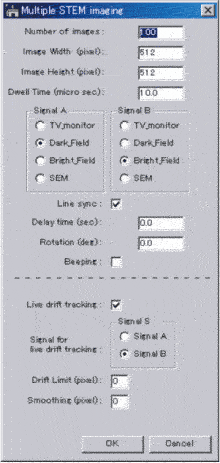
In our previous works, we improved the energy resolution in EELS using software-based techniques such as drift correction and deconvolution. On the basis of these techniques for EELS, we also developed related software techniques for STEM, because the two methodologies are based on the same convolution model. We have prepared several software using Script in DigitalMicrograph (Gatan, Inc.).
High-precision analysis of crystal structure
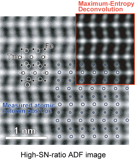
We demonstrate local crystal structure analysis based on ADF/BF imaging in STEM. Using a stabilized STEM instrument and customized software, we first realize high accuracy of elemental discrimination and atom-position determination with less than 10-pm-order accuracy, which can reveal major cation displacements associated with a variety of material properties, e.g. ferroelectricity and colossal magnetoresistivity.
M. Saito, K. Kimoto et al. J. Electron Micrsc. 58 (2009) 131.
K. Kimoto, et al. Ultramicroscopy, 110 (2010) 778-782..
High-sensitivity analysis of Eu-dopants in SiAlON light-emitting phosphor
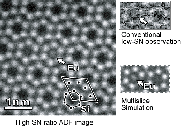
We directly observe a single Eu dopant atom in phosphor beta-SiAlON (specimen; NIMS Hirosaki & Xie) using ADF and BF STEM imaging. A STEM ADF image reveals that a Eu dopant exists in a continuous atomic channel in a beta-Si3N4 structure. The image contrast of the single Eu dopant is confirmed based on the comparison of experimental and simulation results.
Spatially-resolved diffractometry with atomic column resolution
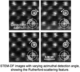 Recent progress in the instrumentation of STEM allows us to acquire various signals from a specimen as a function of probe position. We have demonstrated spatially-resolved diffractometry, in which diffraction patterns are acquired at two-dimensional positions using STEM, resulting in four-dimensional (4D) data. It gives us fundamental knowledge related to STEM imaging techniques, including bright-field (BF), annular dark-field (ADF) and annular bright field (ABF) imaging, because we can construct these images using a single 4D data after the experiment. For instance, we found Rutherford-scattering feature in STEM-DF imaging.
K. Kimoto and K. Ishizuka Ultramicroscopy 111(2011) 1111.