High-mobility p-channel wide-bandgap transistors based on diamond
Diamond has excellent wide bandgap semiconductor properties and therefore could potentially be used to create power electronics and communications devices capable of operating more energy efficiently at higher speeds, voltages and temperatures.
A number of R&D projects have previously been carried out with the aim of creating field-effect transistors (FETs) using hydrogen-terminated diamonds (i.e., diamonds with their superficial carbon atoms covalently bonded with hydrogen atoms).
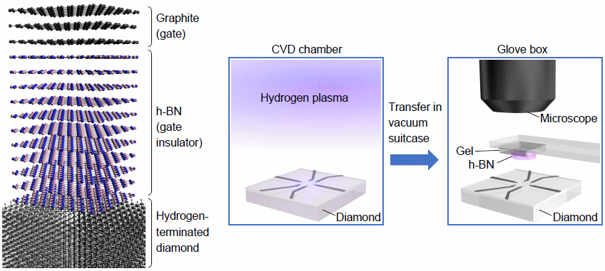
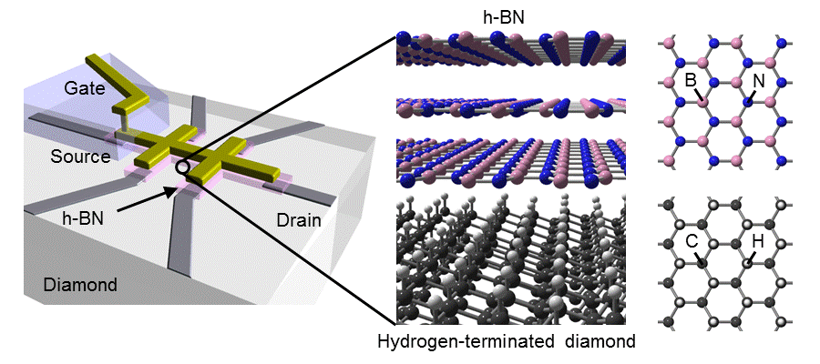
We succeeded in developing a high-performance diamond FETs by using hexagonal boron nitride (h-BN) as a gate insulator instead of conventionally used oxides (e.g., alumina), and by employing a new fabrication technique capable of preventing the surface of hydrogen-terminated diamond from being exposed to air.
Sasama et al. "High-mobility p-channel wide-bandgap transistors based on hydrogen-terminated diamond/hexagonal boron nitride heterostructures"
Nature Electronics 5, 37 (2022); SharedIt view-only PDF; arXiv:2102.05982
Mobility of diamond field-effect transistors
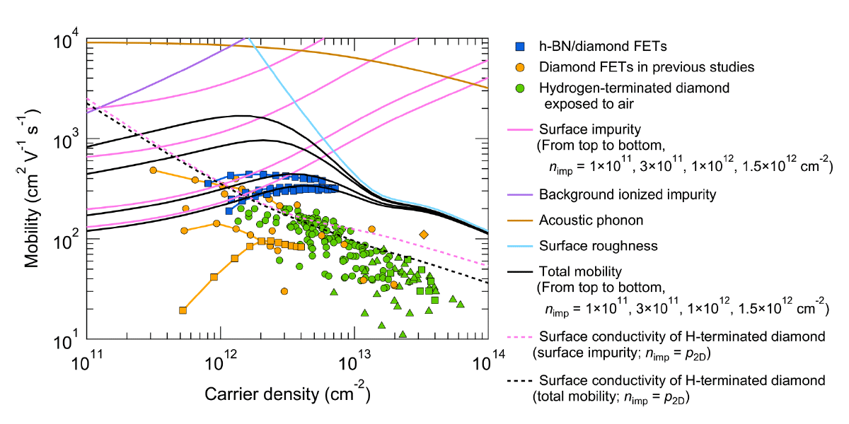
Diamond field-effect transistors (FETs) have potential applications in power and high-frequency electronics. In such applications, high charge-carrier mobility is desirable for a reduced loss and high-speed operation.
We recently fabricated high-mobility diamond FETs with a hexagonal-boron-nitride gate dielectric. A high mobility of 300 cm2V-1s-1 was observed at room temperature, but it was still lower than the phonon-limited intrinsic mobility of diamond.
In this study, we identify the scattering mechanism that limits the mobility of our FETs through theoretical calculations. Our calculations reveal that the dominant carrier scattering is caused by surface charged impurities with a density of ~1012 cm-2, and suggest that an increase in mobility over 1000 cm2V-1s-1 is possible by reducing these impurities.
Sasama et al. "Charge-carrier mobility in hydrogen-terminated diamond field-effect transistors"
Journal of Applied Physics 127, 185707 (2020); arXiv:2001.11831
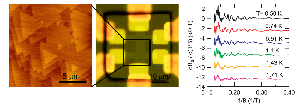
Quantum oscillations in diamond field-effect transistors with a h-BN gate dielectric
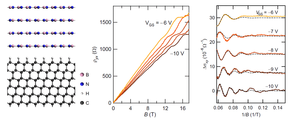
We observed quantum oscillations in diamond field effect transistors fabricated with monocrystalline h-BN as a gate dielectric. The oscillations were observed in both the longitudinal and Hall resistivities, and their frequencies clearly depended on the gate voltage.
Our results indicate the presence of a high-quality two-dimensional hole gas at the diamond surface, paving the way for studies of quantum transport in diamond as well as practical device applications.
Sasama et al. "Quantum oscillations in diamond field-effect transistors with a h-BN gate dielectric"
Physical Review Materials 3, 121601(R) (2019); arXiv:1907.13500
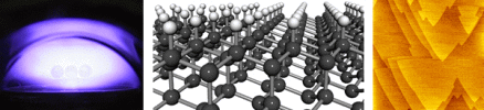
Development of high-mobility diamond transistors with an h-BN gate dielectric
Cleaved monocrystalline hexagonal boron nitride (h-BN) is known as an excellent substrate for graphene as it contains a low density of charged impurities and has a flat surface with no dangling bonds, which helps to improve the mobility of charge carriers in graphene.
By using a monocrystalline h-BN as a gate dielectric, we have successfully fabricated high-performance diamond field-effect transistors. Unprecedentedly high mobilities of charge carriers exceeding 300 cm2V-1s-1 are obtained for moderately high carrier densities (> 5 x 1012 cm-2) at room temperature.
h-BN endures high temperature above 1000 degrees centigrade and its thermal conductivity is comparable to copper at room temperature. Therefore, h-BN is an excellent insulating material for diamond devices that have potential applications in high-temperature and high-power electronics.
Sasama et al. "High-mobility diamond field effect transistor with a monocrystalline h-BN gate
dielectric"
APL Materials 6, 111105 (2018) (open access)
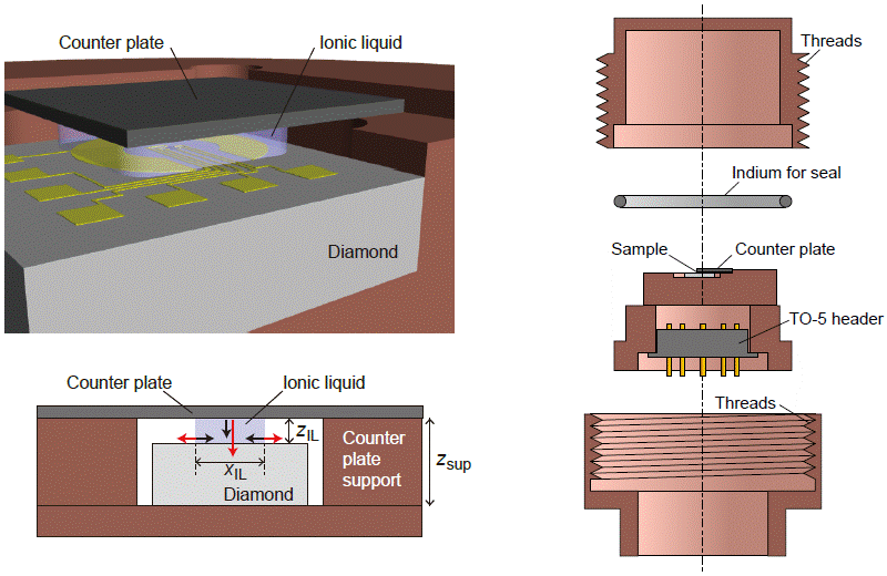
Stable measurements of ionic liquid-gated transistors at low temperatures
Field-effect transistors with ionic liquid as a gate dielectric allow us to obtain the charge carrier density as high as 1014 cm-2 with a low gate voltage. Therefore, it has attracted great attention as a tool that can be used to tune the properties of a material drastically. For example, an insulator-to-superconductor transition can be induced in some materials by changing the carrier density with this technique.
Cooling the transistor is required to observe such a transition, but it sometimes causes a problem: ionic-liquid gated field-effect transistors are often fragile upon cooling. This is presumably due to the shear strain caused by the large difference in the thermal expansion coefficient between the frozen ionic liquid and target sample.
We have developed an experimental technique that suppresses the shear strain and leads to stable measurements on the transistors at low temperatures. The cooling-induced contraction of frozen ionic liquid is compensated for in a mechanical manner using a counter plate and its support. This technique has been developed for the study of diamond and silicon, but it will be used for a wide range of materials and allow stable and efficient measurements at low temperatures.
Yamaguchi et al. "Ionic-liquid-gating setup for stable measurements and reduced electronic inhomogeneity at low temperatures"
Review of Scientific Instruments 89, 103903 (2018); arXiv:1806.09863
Spin-induced anomalous magnetoresistance at the (100) surface of diamond
We found an anomalous positive magnetoresistance at the (100) surface of diamond, which contrasted with the negative magnetoresistance for the (111) surface. The magnetoresistance is orders of magnitude larger than that of the classical orbital magnetoresistance and is nearly independent of the magnetic field orientation.
The in-plane magnetoresistance curves at different temperatures collapse onto a single curve when they are plotted as a function of (magnetic field)/(temperature). These results indicate that the spins of the conductive holes play an essential role at the (100) diamond surface, which may have implications for the development of diamond-based spintronics.
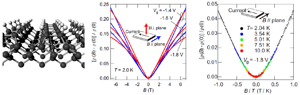
Yamaguchi et al. "Spin-induced anomalous magnetoresistance at the (100) surface
of hydrogen-terminated diamond"
Physical Review B 94, 161301(R) (2016); arXiv:1605.05035
Quantum oscillations (Shubnikov-de Haas oscillations) in diamond
A metallic state of diamond can be induced by heavy boron doping, but the critical dopant concentration is 2-3 orders of magnitude larger than those for Ge and Si. Due to the significant carrier scattering caused by such a large dopant concentration, the carrier mobility is too low for quantum (Shubnikov-de Haas) oscillations to be observed. Unlike doped Ge and Si, Shubnikov-de Haas oscillations have not been reported for doped diamond.
We prepared atomically flat hydrogen-terminated (111) surfaces of diamond and made high-density hole carriers to accumulate at the surfaces using an ionic-liquid-gated field-effect-transistor (FET) technique. This enabled us to obtain a high-mobility metallic state, for which we observed quantum (Shubnikov-de Haas) oscillations in diamond for the first time.
The quantum oscillations depend only on the magnetic field component perpendicular to the diamond surface, thus providing evidence of two-dimensional Fermi surfaces. The effective masses estimated from the temperature dependence of the oscillations are close to the cyclotron effective masses of the valence band maxima in diamond. The estimated scattering time indicates that the carrier mobility is locally as high as several thousand cm2/Vs at low temperature. The high-mobility metallic state of diamond demonstrated here will open up rich fields of research from fundamental physics to device applications.
Yamaguchi et al. "Quantum oscillations of the two-dimensional hole gas at atomically flat diamond surfaces"
Physical Review B 89, 235304 (2014)
Electric field-induced insulator-metal transition of diamond
Electronic applications of diamond have been anticipated in various fields owing to its excellent properties. As pure diamond is an insulator, the introduction of charge carriers is important for electronic applications. The most common method to introduce charge carriers is chemical doping. Heavy boron doping of diamond can induce a metallic state, and even a superconducting state at low temperature. However, carrier scattering due to the high-density dopants leads to a very low mobility. It is also predicted that the superconducting transition temperature would be suppressed by the electronic disorder due to the heavy doping.
An alternative clean approach for introducing carriers is to use the electric field effect. We fabricated an field effect transistor on the hydrogen-terminated surface of diamond and investigated the transport properties of carriers that are made to accumulate at the surface. We used an ionic liquid as a gate dielectric to introduce high density carriers with a low gate voltage.
At zero gate voltage, the sheet resistance increases with decreasing temperature, indicating an insulating state. The application of negative gate voltage allows the hole carriers to accumulate at the surface and hence decreases the resistance. At the gate voltage of -1.6 V, the resistance is nearly independent of temperature, which indicates metallic carrier transport. Thus, we observed an insulator-metal transition of diamond induced by the electric field effect for the first time. The mobility of the carriers in this metallic state is much larger than that of boron-doped diamond with a similar resistivity.
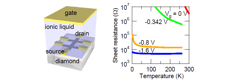
Yamaguchi et al. "Low-Temperature Transport Properties of Holes
Introduced by Ionic Liquid Gating in Hydrogen-Terminated Diamond Surfaces"
Journal of the Physical Society of Japan 82, 074718 (2013)