後藤 敦 Atsushi Goto

Group Leader/Chief Researcher
Solid-state NMR Group, Center for Basic Research on Materials,
High Magnetic Field Characterization Unit, Adv. Eng. & Services Division
E-mail:GOTO.Atsushi=nims.go.jp
(Please replace [=] with [@] )
Research Overview
- R&D of Solid-State NMR in Materials Science
- R&D of Hyperpolarization Schemes for semiconductors
Keywords
NMR, Hyperpolarization, Optical Pumping, High Magnetic Fields
Profile
Dr. Goto received his Ph.D. in Science from the Department of Physics (Institute for Solid State Physics), The University of Tokyo in 1996 under the supervision of Prof. Hiroshi Yasuoka, with a thesis titled "NMR Studies of the Spin Gap Anomalies in High-Tc Cuprates." Shortly thereafter, he joined National Research Institute for Metals (now NIMS), where he was engaged in projects related to superconducting materials (Superconducting Materials Multicore Project, MEXT) and quantum computing (CREST, JST). In 2000, he conducted high-field NMR research at UCLA on sabbatical leave. He concurrently served as a JST PRESTO researcher from 2007 to 2011, and has been in his current position since 2020.
Research & Achievements
Research expertise encompasses condensed matter physics, materials science, and materials characterization. The research focuses on pioneering advanced measurement technologies such as high-field NMR and optical pumping NMR, aiming at the elucidation of local electronic states in strongly correlated electron systems, sensitivity enhancement via nuclear hyperpolarization techniques, and the application of solid-state nuclear spins to quantum information processing. Notably, he has pursued the establishment of unique measurement methodologies merging optics and NMR, such as developing nuclear spin polarizers via optical pumping and controlling optically-induced nuclear spin interactions in semiconductors. With over 100 papers in leading international journals, including Physical Review Letters, Nature Communications, and Review of Scientific Instruments, he has led numerous projects supported by JST, NEDO, and JSPS-KAKENHI as a principal investigator.
Professional Activities & Awards
In parallel with research activities, he is engaged in the solid-state NMR user facility operations at NIMS to analyze diverse advanced materials from both within and outside the institute, while also serving as a reviewer for major international journals, including Physical Review Letters, and as an expert reviewer at funding agencies such as NEDO and KAKENHI. In 2015, he was co-awarded the NIMS President's Award for technological developments that contributed to achieving a world record in high-field NMR magnets.
[Research Topic]Optical Pumping NMR and Optically Induced Nuclear Spin–Spin Couplings in Semiconductors: Double Resonance NMR Experiments under Light Illumination
ー Overview ー
A quantum computer is a new computational concept that utilizes the principles of quantum mechanics. It is expected to solve problems that are virtually unsolvable with current computers due to the extremely long computation times required. The solid-state NMR quantum computer uses nuclear spins in solids (mainly semiconductors) as quantum bits, and is considered one of the promising approaches for realizing a "large-scale" quantum computer. However, a key challenge in this approach is the development of methods to manipulate the "nuclear spin interactions," which are responsible for transmitting information between quantum bits. In this study, we have discovered that nuclear spin interactions in semiconductors can be controlled in a simple manner by turning the light on and off. This finding is expected to contribute to the realization of solid-state NMR quantum computers.
ー Introduction ー
NMR quantum computers are a type of quantum computer that use nuclear spins in matter as quantum bits, and have been actively studied since the dawn of quantum computer research. One of the major challenges in realizing quantum computers is how to integrate a large number of qubits and thereby perform large-scale computations (scalability). In this context, semiconductors are regarded as promising platforms for scalable NMR quantum computers. This is due to unique characteristics of semiconductors, such as the well-established nanofabrication technology suitable for constructing architectures, and a long decoherence time (*1) stemming from the long nuclear spin relaxation times on the order of several hours [1]. Furthermore, the optical control of nuclear spins is also an important factor. By using the so-called “optical pumping NMR method” described below, it is possible to generate a hyperpolarized nuclear spin state (*3) that functions as an initialized (*2) nuclear spin qubit [2,3]. An advantage of this technique is that, after initialization is complete, photon-excited electrons—which could be sources of noise—can be easily eliminated simply by switching off the light. In addition, the ability to realize “two-qubit operations,” which are essential for quantum computation, using light is another major feature of semiconductor-based NMR quantum computers.
(*1) The time limit for which quantum superposition (coherence) can be maintained. Longer times are more favorable, as they allow for longer computation durations.
(*2) Resetting all qubits to the zero state before beginning a quantum calculation; comparable to the “setting to zero” operation in an abacus.
(*3) A phenomenon where the orientation of many nuclear spins becomes aligned beyond the thermal equilibrium state, enabling ultra-sensitive NMR measurements.
Two-qubit operations use interactions between nuclear spins (nuclear spin–spin coupling) [1,4,5,6,7]. There are two types of nuclear spin–spin coupling: direct (nuclear dipolar) coupling and indirect (electron-mediated) coupling. In conventional solution-state NMR quantum computers, direct coupling has mainly been used. However, since this interaction is always present, it is necessary to control it using techniques such as dipolar decoupling or recoupling in order to turn off two-qubit gates [7]. On the other hand, because indirect coupling is mediated by electrons, it is expected that the strength of this interaction can be controlled by manipulating the electronic states. Notably, in semiconductors, there are nominally no free electrons to mediate the coupling, so indirect coupling is naturally off by default; by generating electrons optically, it becomes possible to control the coupling on and off. This interaction, called “optically induced nuclear spin–spin coupling,” brings new advantages to semiconductor-based NMR quantum computers [8,9].
The existence of optically induced nuclear spin–spin coupling was first demonstrated in cross polarization (CP) experiments under optical pumping in a typical compound semiconductor, gallium arsenide (GaAs) [8], and was later confirmed by spin echo double resonance (SEDOR) experiments [9]. In the SEDOR experiment, changes in the echo decay rate were observed under light irradiation, which have been interpreted as resulting from changes in heteronuclear spin–spin coupling. Both CP and SEDOR methods are double-resonance NMR techniques that provide information about the coupling between hyperpolarized nuclear spins.
Here, we provide an overview of the optical effects on nuclear spin systems in semiconductors, and introduce double-resonance NMR experiments used to elucidate their properties. For details of the experiments described here, please refer to references [8,9]. For details of the experimental setup, please see reference [10].
ー Optically Induced Effects on Nuclear Spins in Semiconductors ー
(1) Optical pumping NMR
Since the French physicist G. Lampel first discovered the underlying phenomenon [11], optical pumping NMR has attracted much attention as an effective method for achieving "hyperpolarization" in the world of semiconductors, and is now widely used. Below, we briefly explain how optical pumping NMR occurs [2,3].
First, when circularly polarized light with energy matching the band gap of the semiconductor (light with a “rotating” property) is irradiated onto the sample, electrons jump from the valence band to the conduction band (especially at a location called the Γ point). The electrons that enter the conduction band have aligned spins, which is referred to as "electron polarization." Although these excited electrons do not last long and quickly disappear, if the temperature is sufficiently low (below several tens of kelvin), a net spin polarization remains while the electrons exist, and this polarization is transferred to the nuclear spins. However, in this polarization transfer process, the optically excited electrons are not finely controlled, so the transfer of spin polarization proceeds rather slowly. Therefore, it usually takes several minutes or even several hours to polarize the nuclear spins. For comparison, in dynamic nuclear polarization (DNP) methods that use microwaves to actively control electron spins, the polarization transfer proceeds much faster.
Figure 1 shows an example of optical pumping NMR observed in undoped GaAs (GaAs without impurities). In the experiment, right-circularly polarized light with energy matching the band gap of GaAs (about 1.5 eV) is irradiated at a low temperature of 10 K, and then the signal from Ga-71 is measured. The Ga signal in NMR appears strongly in the negative direction, indicating that the nuclear spins are aligned in the opposite direction to the thermal equilibrium state.
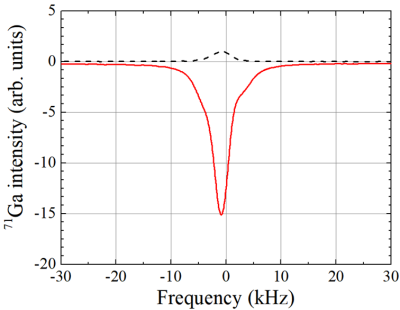
Fig. 1. Solid line: Optical pumping NMR spectrum of 71Ga measured in undoped GaAs after irradiation with infrared light (σ+, 826 nm, 120 mW) for 2 minutes. Frequency: 121.9762 MHz, magnetic field: 9.39 T, temperature: 10 K. Dashed line: Spectrum without light irradiation.
(2) Optically induced nuclear spin-spin couplings
Optically induced nuclear spin–spin coupling appears, like optical pumping, when light with energy near the band gap of the semiconductor is irradiated [8,9]. As the power of the light increases, the coupling becomes stronger and its influence extends farther. In the world of metals, such indirect coupling is known as "Ruderman–Kittel-type interaction" [12], which features a coupling strength that oscillates (varies like a wave) depending on the distance between two nuclear spins. The optically induced coupling exhibits similar characteristics; interestingly, however, the “oscillation period” in this case changes according to the power of the light.
ー Double Resonance Experiments Under Light Irradiation ー
(1) Cross Polarization (CP) Experiments Under Light Irradiation
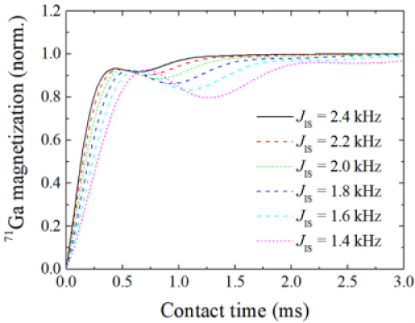
Optically induced nuclear spin–spin coupling was first discovered in cross polarization (CP) experiments conducted between 71Ga nuclei and 75As nuclei in undoped GaAs under optical pumping conditions [8]. With 60 seconds of light irradiation, the optical pumping effect accumulates the spin polarization of the 75As nuclei. This polarization is then transferred to the 71Ga nuclei via a cross polarization process (*4) performed under light irradiation. During this process, the polarization of the 71Ga nuclei oscillates depending on the contact time (*5), and the position of the peak shifts toward shorter contact times as the light power increases. In simple terms, the timing at which the peak appears corresponds to a time known as the cross relaxation time, which is closely related to heteronuclear indirect coupling.
(*4) Adjusting the effective “resonance frequency = energy” of two types of nuclear spins so that they can interact with each other.
(*5) The period during which the cross polarization state is maintained. During this time, the two types of nuclear spins are in thermal "contact."
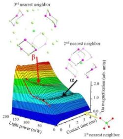
Figure 2(a) shows a simple simulation of such transient oscillations. The stronger the heteronuclear coupling, the more the oscillation peaks shift toward shorter contact times. Figure 2(b) shows actual experimental data. As the light power increases, multiple peaks appear sequentially, and their positions also shift toward shorter contact times. These peaks correspond to specific groups of atoms, such as first nearest neighbors, second nearest neighbors, and so on (c). From these results, it can be seen that the range of the optically induced nuclear spin–spin coupling expands as the light power increases.
-
(a) -
.png)
(b) -
(c)
Fig. 2 (a) Simple simulation of the cross polarization experiment in GaAs with varying heteronuclear coupling (JIS). For simplicity, the correlation time of CP is assumed to be constant. (b) Contact time dependence of 71Ga magnetization in the cross polarization (CP) experiment. Measurements were performed at 10 K, varying the irradiated light power from 0 to 200 mW. The black, red, and blue arrows each indicate three series of maxima. (c) Three-dimensional representation of the interpolated experimental data from Figure 2(b). The data indicated by the yellow arrow corresponds to the case without light irradiation, representing polarization transfer to nearest neighbor atoms due to conventional spin–spin coupling. The black (α) and red (β) arrows each indicate series of maxima corresponding to polarization transfer to the second and third nearest neighbor sites, respectively. The dashed line shows the 71Ga magnetization at a contact time of 0.7 ms, where a plateau-like (i.e., the slope becomes gentler) feature appears near 80 mW. (Figs. (b) and (c) are reproduced from Ref. [8] under the terms of the CC BY 4.0 license.)
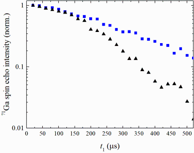
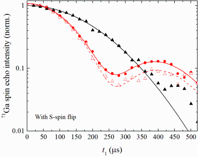
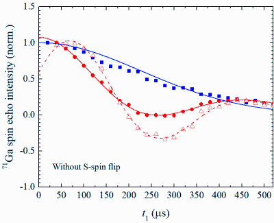
(2) Spin Echo Double Resonance (SEDOR) Experiments Under Light Irradiation
To reveal the overall picture of optically induced nuclear spin–spin coupling, we performed spin echo decay experiments under light irradiation [9]. Spin echo decay measurements are a technique used to detect the strength of interactions between nuclear spins. In standard spin echo decay measurements, a two-pulse (Hahn echo) sequence—corresponding to 90° and 180° pulses—is applied to a single nuclear species (in this case, gallium nuclei: 71Ga). In contrast, in SEDOR experiments, a 180° pulse (P3) is also applied to arsenic nuclei (75As) at the same timing as the 71Ga pulse sequence. In the absence of the P3 pulse (standard spin echo decay measurement), only couplings between 71Ga nuclear spins contribute to echo decay, but when the P3 pulse is applied, couplings between 71Ga nuclear spins as well as heteronuclear interactions between 75As and 71Ga also contribute to the echo decay [13]. In other words, the P3 pulse acts as a switch that can turn on or off the coupling between different nuclear species (75As and 71Ga), and by comparing the cases with and without the P3 pulse, the effects of homonuclear and heteronuclear couplings can be distinguished.
In the experiment, echo decay was measured at two different light power intensities and compared to that without light irradiation. Figure 3 shows an example of the SEDOR experiment performed under light irradiation. Oscillations in the echo peak intensity with respect to the delay time (the wait time between pulses: t1) were also observed, which are attributed to quadrupolar interactions and are not directly related to echo decay. Therefore, the influence of these oscillations was considered when determining accurate decay times (T2).
From the results of the SEDOR experiments (Figure 3(b)), it was found that the echo decay rate (1/T2) decreases as the light power increases. This indicates that the total coupling strength between homonuclear and heteronuclear spins becomes weaker. On the other hand, in the standard Hahn echo decay experiment (Figure 3(c)), the change in 1/T2 was small, indicating that the coupling between 71Ga nuclei remains almost unchanged. In other words, the decrease observed upon increasing the light power is mainly due to a reduction in heteronuclear coupling (71Ga - 75As).
Combining these results with the findings from the previously discussed CP experiment [8], it can be concluded that, within this range of light power, the induced coupling primarily affects only the nearest neighbor 75As nuclei. Moreover, the reduction in heteronuclear coupling (71Ga - 75As) is due to the optically induced coupling and the original dipolar coupling canceling each other out, indicating that these two couplings have opposite signs (directions).
-
(a) -
(b) -
(c)
Fig. 3 (a) Semi-log plot of the normalized spin echo decay process measured in the absence of light irradiation, with and without the S spin inversion (P3) pulse (with: ▲, without: ■) (10 K, repetition time: 20 minutes). (b), (c) Normalized spin echo decay processes measured under light irradiation, with (b) and without (c) the S spin inversion (P3) pulse, as well as the non-irradiated data shown in (a) (10 K, irradiation time: 5 minutes). ● and Δ indicate measurements at light intensities of approximately 173 mW/cm² and 346 mW/cm², respectively. Note that the vertical axis in (c) is displayed on a linear scale. (Reprinted from Ref. [9] under the terms of the CC BY 4.0 license.)
ー Summary ー
Here, we introduced two optical effects on nuclear spin systems in semiconductors: hyperpolarization via optical pumping and optically induced nuclear spin-spin coupling. Both effects manifest when light with energy corresponding to the band gap is irradiated. These two phenomena are expected to play important roles in realizing scalable NMR quantum computers based on semiconductors. We also showed that double resonance NMR experiments such as CP and SEDOR are effective for elucidating the properties of optically induced coupling. Double resonance NMR can be regarded as a powerful technique for investigating interactions between nuclear spins in detail.
ー Acknowledgments ー
This research was partially supported by JSPS KAKENHI grants.
ー References ー
[1] B.E. Kane: Nature 393 , 133 (1998).
[2] R. Tycko and J. A. Reimer: J. Phys. Chem. 100, 13240 (1996).
[3] S. E. Hayes, S. Mui and K. Ramaswamy: J. Chem. Phys. 128, 052203 (2008).
[4] I. L. Chuang, N. Gershenfeld and M. Kubinec: Phys. Rev. Lett. 80, 3408–3411 (1998).
[5] J. A. Jones, and M. Mosca: J. Chem. Phys. 109, 1648 (1998).
[6] L. M. K. Vandersypen, M. Steffen, G. Breyta, C. S. Yannoni, M. H. Sherwood and I. L. Chuang: Nature 414, 883 (2001).
[7] A. Goto, T. Shimizu, K. Hashi, H. Kitazawa and S. Ohki: Phys. Rev. A 67, 022312 (2003).
[8] A. Goto, S. Ohki, K. Hashi and T. Shimizu: Nat. Commun. 2, 378 (2011).
[9] A. Goto, S. Ohki, K. Hashi and T. Shimizu: npj Quant. Inf. 8, 59 (2022).
[10] A. Goto, S. Ohki, K. Hashi and T. Shimizu: Jpn. J. Appl. Phys. 50, 126701 (2011).
[11] G. Lampel: Phys. Rev. Lett. 20, 491 (1968).
[12] M. A. Ruderman and C. Kittel: Phys. Rev. 96, 99 (1954).
[13] C. P. Slichter: Principles of Magnetic Resonance (Springer-Verlag, Berlin, 1990) 3rd ed., Chap. 7.21, p. 311.
This page is based on the following article, with some parts omitted and reorganized:
A. Goto et al., "Optical Pumping NMR and Optically Induced Nuclear Spin–Spin Couplings in Semiconductors: Double Resonance NMR Experiments under Light Illumination", JPS Conf. Proc. 38, 011185 (2023), DOI:10.7566/JPSCP.38.011185.
This work is licensed under a Creative Commons Attribution 4.0 International License (CC BY 4.0).
Note: Parts of Figs 2 and 3 are reproduced from references [8] and [9], respectively, as indicated in each caption.