NIMS Award 2026 Winners have been selected!
NIMS (National Institute for Materials Science) has decided to present the NIMS Award 2026 to Prof. Ryoji Kanno from the Institute of Science Tokyo and Prof. Masahiro Tatsumisago from Osaka Metropolitan University. They brought about significant innovations to“all-solid-state batteries”in a field which in recent years has seen an intensifying of global competitions toward next-generation energy storage technologies.
Prof. Ryoji Kanno and Prof. Masahiro Tatsumisago pioneered the path leading to high-performance all-solid-state batteries through the development of sulfide-based ion-conducting solid materials and the elucidation of their conduction mechanisms.
Prof. Kanno paved the way for crystalline solid electrolytes exhibiting high ionic conductivity, whereas Prof. Tatsumisago pioneered the development of amorphous solid electrolytes. These achievements have led to industrial applications, including automotive batteries and stationary energy storage systems, as a key technology for realizing safe and high-energy-density next-generation batteries, and have become an important technological foundation for achieving a carbon-neutral society. Both have made worldwide impacts on all-solid-state battery research and its practical applications, as befit the aim of the NIMS Award 2026.
The ceremony and recipients’ lectures for the NIMS Award 2026 will take place during the “NIMS Award Symposium 2026 - Engineering the Future of Solid State Batteries” to be held on Tuesday, November 10 at the Tsukuba International Congress Center.
Pioneering research on solid electrolytes enabling all-solid-state batteries
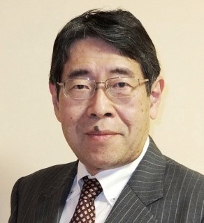
Prof. Ryoji Kanno
Institute Professor
Institute of Science Tokyo

Prof. Masahiro Tatsumisago
Executive Advisor
Osaka Metropolitan University
Research Summary and Impact on the Academic and Industrial Sectors
Research Summary
The work of the awardees has made comprehensive and pioneering contributions to realizing all-solid-state batteries, which is a key technology in next-generation energy storage, through the development of sulfide-based ion-conducting solid materials and the elucidation of their conduction mechanisms.
Prof. Ryoji Kanno developed crystalline sulfide solid electrolytes, including Li₁₀GeP₂S₁₂ (LGPS) and argyrodite-type materials, achieving superionic conductivity at room temperature that significantly exceeds that of conventional liquid electrolytes. Furthermore, he advanced the understanding of lithium-ion diffusion pathways based on studies of crystal structures and defect chemistry, and established guidelines for designing materials exhibiting high ionic conductivity.
Prof. Masahiro Tatsumisago pioneered amorphous and metastable crystalline materials exhibiting fast ion conduction through the development of ion-conducting glasses and glass-ceramics typified by the Li₂S–P₂S₅ system, thereby establishing a materials foundation for the practical application of sulfide-based solid electrolytes.
Together, their complementary approaches—spanning amorphous to crystalline materials—established comprehensive principles for achieving fast ionic conduction and advanced the understanding of electrode/electrolyte interfaces. These achievements have laid the scientific and technological foundation for high-performance all-solid-state batteries.
Impact on the Academic and Industrial Sectors
The combined contributions of Prof. Kanno and Prof. Tatsumisago have transformed the field of solid-state ionics and energy materials science by integrating seemingly opposing approaches incorporating crystalline and amorphous solids into a unified framework for ion conduction. Their work has significantly advanced the fundamental understanding of fast ion transport and stimulated extensive global research activities, as reflected in the high citations of their publications.
From an industrial perspective, their discoveries have triggered the development of sulfide-based all-solid-state battery technologies, which are being actively studied for applications in electric vehicles, grid-scale energy storage, and portable electronics. Their work has provided essential materials and design guidelines that have accelerated industrial R&D worldwide.
By enabling safer and higher energy-density battery systems, these achievements are expected to play a crucial role in advancing next-generation energy technologies and contribute to the realization of a carbon-neutral society.
■Glossary
(1) All-solid-state battery: a next-generation battery that uses solid materials as electrolytes, offering high safety and high energy density.
(2) Sulfide-based materials: materials containing sulfur as a main component, known for their high ionic conductivity in all-solid-state batteries.
(3) Solid electrolyte: a solid material that conducts ions and enables ion transport between electrodes in all-solid-state batteries.
(4) Amorphous material: a material in which atoms are not arranged in a regular, ordered structure.
(5) Crystalline material: a material with a regularly ordered crystal structure of atoms.
NIMS Award Committee 2026
- ■External Committee Members
Akitoshi Hayashi (Professor, Graduate School of Engineering, Osaka Metropolitan University)
Yasutoshi Iriyama (Professor, Graduate School of Engineering Science, Nagoya University)
Shinichi Orimo (Professor,Advanced Institute for Materials Research, Institute for Materials Research, Tohoku University)
Junichiro Shiomi (Professor, Graduate School of Engineering, The University of Tokyo)
Shohji Tsushima (Professor, Graduate School of Engineering, Osaka University)
- ■Internal Committee Members (NIMS)
Takashi Taniguchi (Executive Vice President in charge of the NIMS Award, Chair of the Selection Committee)
Masayuki Takeuchi(Executive Vice President)
Hideo Hosono(Distinguished Fellow, Research Center for Materials Nanoarchitectonics (MANA) Team Leader)
Kazunori Takada (Fellow, Research Center for Energy and Environmental Materials (GREEN))
Takuya Masuda (Director, GREEN)
Koji Kamiya (Deputy Director,GREEN)
Hiroyo Segawa (Deputy Director, Research Center for Electronic and Optical Materials)
Kazutaka Mitsuishi (Deputy Director, Center for Basic Research on Materials)
Hitoshi Ota (Platform Director, GREEN)
Naoaki Kuwata (Group Leader, GREEN Solid State Battery Ionics Group)
Toshihiko Mandai (Group Leader, GREEN Frontier Battery Materials Group)
Shogo Miyoshi, (Senior Researcher, GREEN Solid-State Battery Group)
Kei Kubota (Senior Researcher,Battery Materials Analysis Group)
NIMS Award Symposium 2026
NIMS Award Ceremony and Commemorative Lecture
at Tsukuba International Congress Center
November 10th, 2026