Research
Research
1.Ionic Nanoarchitectonics
Solid-state ion devices operate by controlling the movement of ions and electrochemical phenomena within solids at nano- and atomic levels using an external voltage. Carefully selecting the type of ion and the interface structure of the material makes it possible to achieve characteristics that are not seen in conventional semiconductor devices. We refer to this technology for controlling ions as “Ionic nanoarchitectonics”.
1.1 Diverse solid-state ionic devices using ionic nanoarchitectonics technology
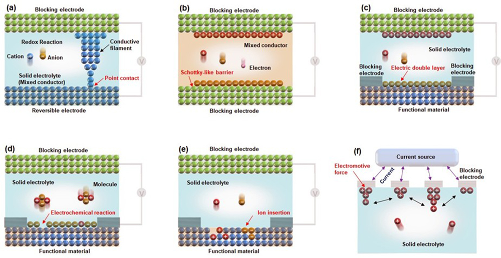
Figure 1 shows the representative device structures and operating principles that we are developing.
The device in Figure 1(a) has a structure in which an ion or mixed conductor is sandwiched between electrodes. Applying a voltage causes conductive filaments to form and dissipate, enabling resistance changes. This has led to the development of quantized conductance atomic switches, non-volatile memory, artificial synapses and radiation-resistant switches.
The device in Figure 1(b) consists of a mixed conductor and an inert electrode. Applying a voltage adjusts the Schottky-like barrier, enabling the device to function as a variable diode, among other roles.
The device in Figure 1(c) is a transistor structure. Applying voltage creates an electric double layer, resulting in electrical properties such as on/off switching and analogue resistance changes.
The device in Figure 1(d) is also a transistor structure. It uses electrochemical reactions to control the adsorption/desorption of surface atoms on functional materials, which enables diverse optical and electrical properties.
The device in Figure 1(e) achieves diverse electrical properties by inserting or extracting ions when voltage is applied.
Figure 1(f) shows a device that uses electrodes on the surface of an ionic conductor to measure accumulated ions via voltage, enabling functions such as learning and memory.
These devices have a layered structure similar to that of conventional semiconductor devices and can be manufactured using the same fabrication process.
2.Atomic Switch
We have created atomic switches that work through the movement of ions and electrochemical reactions at an atomic level. These switches control the formation and disappearance of filaments within solids, through which ions move and electricity flows. We are elucidating this device’s operating principles and exploring its new properties and functions, which are not found in conventional semiconductors.
2.1 Control of ion movement and electrochemical reactions at the atomic scale
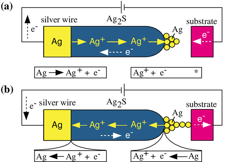
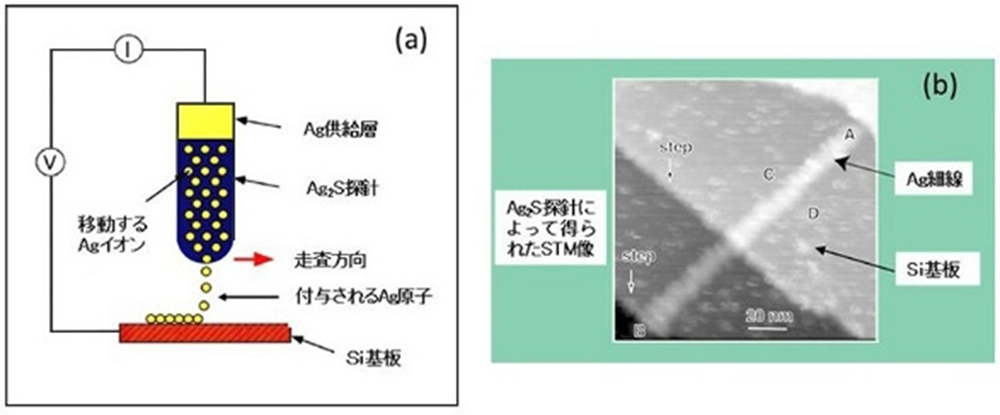
Silver sulfide (Ag₂S) is a unique material that can conduct both silver ions and electrons. We use it as a probe in a scanning tunnelling microscope (STM). By varying the direction and magnitude of the voltage applied between the Ag₂S probe and a platinum substrate, or by altering the current, we can cause tiny silver protrusions to form or shrink at the tip of the probe (Figure 2).
This phenomenon results from an electrochemical reaction occurring within the solid. The distance between the Ag₂S probe and the platinum substrate is very small, at around 1 nanometre (1 nm). Therefore, when a negative voltage is applied to the substrate, tunnelling electrons flow from the substrate towards the probe. At this time, silver ions (Ag⁺) near the tip of the Ag₂S probe are reduced by the electrons and transform into silver atoms (Ag). These unstable silver atoms then migrate to the surface and form protrusions (Figure 2 (a)).
Conversely, when the polarity of the voltage is reversed to positive, tunnelling electrons flow from the silver protrusion at the tip of the probe back towards the substrate. During this process, the silver atoms within the protrusion are oxidized back into ions (Ag⁺) and reintegrate into the Ag₂S. Consequently, the protrusion shrinks and eventually disappears (Figure 2 (b)). It was discovered that an extremely small switch (on/off) can be created by utilizing this phenomenon of enlarging or shrinking the silver protrusions.
2.2 Gap-Type Atomic Switches
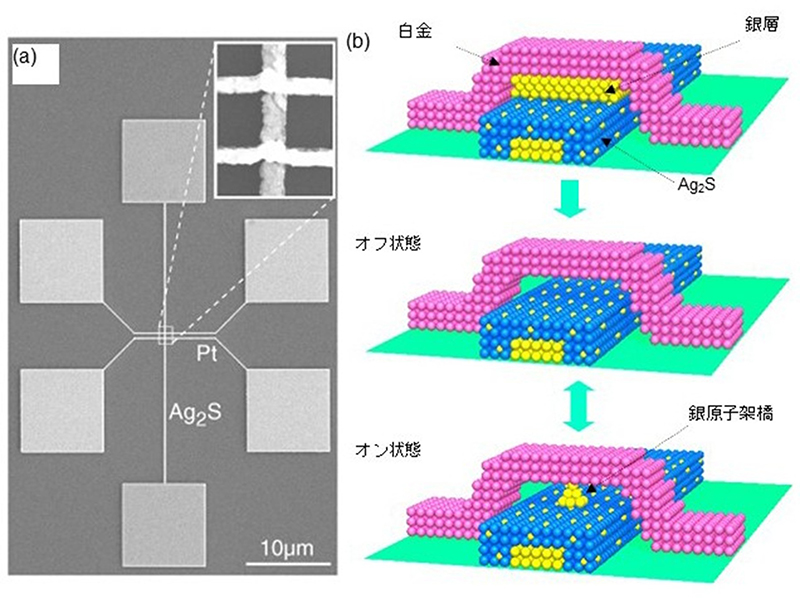
Based on fundamental experiments involving STM tunnelling electrons to control localized ion movement and electrochemical reactions, we developed an ultra-miniature switch device called an ‘atomic switch’, which functions through the movement of several to several dozen atoms (ions). This atomic switch is fabricated using the precise processing techniques employed in semiconductor device manufacturing.
Electron microscope images and structural diagrams of the fabricated atomic switch are shown in Figures 3 (a) and (b). It consists of a crossbar arrangement layered with silver (Ag) and silver sulfide (Ag₂S) wires, an extremely thin silver film (approximately 1 nm thick) and a platinum (Pt) wire (electrode).
In this device, applying a positive voltage to the platinum electrode causes the silver film to oxidize into silver ions. These ions are then incorporated into the Ag₂S wire, resulting in the disappearance of the Ag thin film. This creates a minute gap between the Pt electrode and the Ag₂S wire. In this state, tunnelling electrons flow through the approximately 1 nm gap, but the electrical resistance is high, ranging from several MΩ to tens of MΩ.
Next, applying a negative voltage to the Pt electrode causes tunnelling electrons to flow from the Pt electrode to the Ag₂S filament. When a voltage and current exceeding a certain threshold are applied, the Ag ions contained within the Ag₂S filament are reduced and emerge on its surface as Ag protrusions. This forms an Ag (silver) bridge across the gap, causing the electrical resistance to drop significantly to several kiloohms to tens of ohms (see Figure 3(b)). Furthermore, switching the polarity of the voltage applied to the electrodes back to positive causes the silver bridge to dissolve back into Ag₂S as Ag ions, resulting in the disappearance of the bridge. This enables the gap-type atomic switch to perform on/off switching operations (Figure 4).
2.3 Emergence of Various Functions
Gap-type atomic switches are expected to have a variety of applications beyond simple switching. For instance, they exhibit the unique phenomenon of ‘quantized conduction’, with potential applications in multivalue memory, logic gates for computation, nano-pens, synapse devices and decision-making devices utilizing this mechanism.
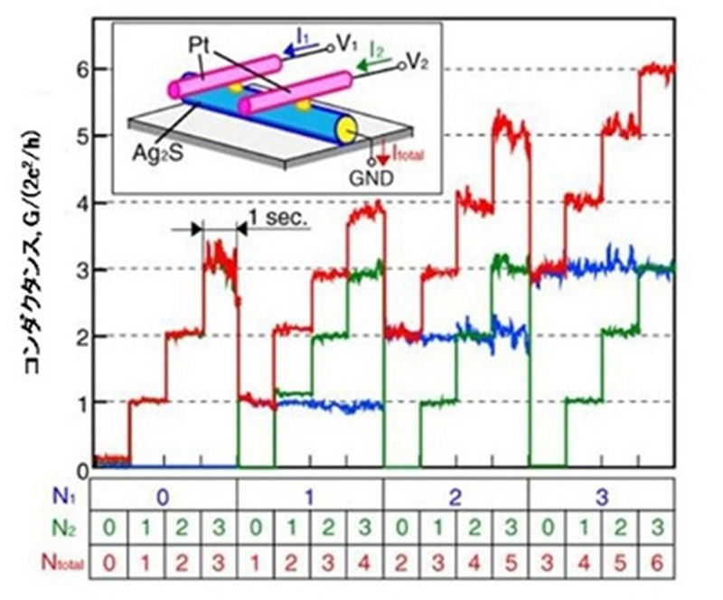
This phenomenon was discovered by carefully adjusting positive and negative voltages to control the tunnelling current and, consequently, the electrochemical reaction. Specifically, in an atomic switch with the structure Ag electrode/Ag₂S/gap/Pt electrode, a very small voltage is applied between the Pt electrode and the Ag electrode to allow a silver (Ag) protrusion to slowly grow. This causes the silver protrusion to grow slowly, eventually forming a ‘point contact’ state where it makes contact with the Pt electrode at a single point. This point contact can be finely tuned at the atomic level, leading to the emergence of a special electrical flow known as quantized conduction. Using this phenomenon enables the creation of multivalue memory, which is memory capable of recording multiple states in a single memory cell.
For instance, an Ag electrode/Ag₂S/gap/Pt electrode array (crossbar structure) can be formed with atomic switches created at two intersection points. Each switch exhibits quantized conduction when the voltage is finely adjusted. Furthermore, applying an appropriate polarity and strength of voltage pulse to this state changes the point contact state, enabling the quantum number (i.e. the quantized conduction stage) to be freely switched. Figure 5 shows two atomic switches side by side, each of which has four states ranging from quantum number 0 to 3, giving a total of 16 possible states. This enables the development of multivalued memory.
Furthermore, “nano pen” technology uses an Ag₂S material scanning tunnelling microscope (STM) probe (Figure 6(a)). By applying an appropriate voltage between the probe and the substrate, Ag atoms can be transferred continuously from the probe tip to the substrate, enabling fine metallic lines to be drawn. Essentially, the STM probe itself becomes the ‘ nano pen”, with Ag ions moving within the Ag₂S acting as the ‘ink’. Using such an ultra-fine nanopen enables the drawing of freely shaped metallic atomic filaments on the sample surface (Figure 6(b), Figure 7).
2.4 Junction (Gapless) type atomic switch
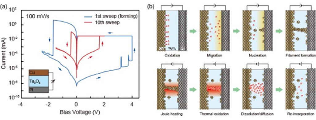
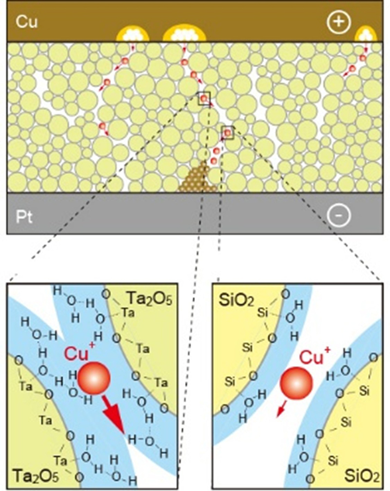
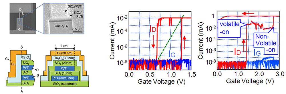
We are investigating the operating mechanism of and developing various functions for junction (gapless)-type atomic switches, based on the formation and dissolution of metal filaments in metal/insulator/metal structure. Using inorganic and organic insulators (Solid electrolytes), we have succeeded in realizing various characteristics, such as microscopic switching mechanisms, fast-switching dynamics, moisture adsorption, quantized conductance, and synaptic behaviors. We have investigated the resistive switching mechanism and unique properties of a metal/insulator/metal (MIM)-structured atomic switches using Ta2O5 as the model matrix. Figure 8 shows the typical I-V characteristics and the corresponding operating mechanism of a Cu/Ta2O5/Pt cell. The cell is SET from the OFF state to the ON state under positive bias relative to the Cu electrode, and is RESET from the ON state to the OFF state under negative bias, indicating bipolar resistive switching behavior, as shown in Figure 8 (a). The SET operation consists of the anodic oxidation of Cu under bias applications, migration of oxidized Cu ions in the Ta2O5 matrix, and nucleation of Cu on the Pt electrode, followed by formation of a metal filament between the two electrodes. The RESET operation is attributed to thermal oxidation of Cu in the filament due to Joule heating and diffusion of Cu ions under ion concentration gradient and an electric field, as illustrated in Figure 8 (b). Repeated redox reactions at Cu(Ag)/Ta2O5 interfaces were observed by Cyclic Voltammetry, and the concentration and diffusion coefficient of the created ions were evaluated. Furthermore, we found that the morphology and deliquescency of Ta2O5 films affects the resistive switching characteristics of the oxide-based atomic switch, as illustrated in Figure 9.
Reference
- [1] T. Tsuruoka et al., J. Electroceram., 39(2017) 143 Operating mechanism and resistive switching characteristics of two- and three-terminal atomic switches using a thin metal oxide layer | Journal of Electroceramics | Springer Nature Link
- [2] T. Tsuruoka et al., Adv. Funct. Mater., 22(2012) 70 https://doi.org/10.1002/adfm.201101846
2.5 Polymer-based atomic switch
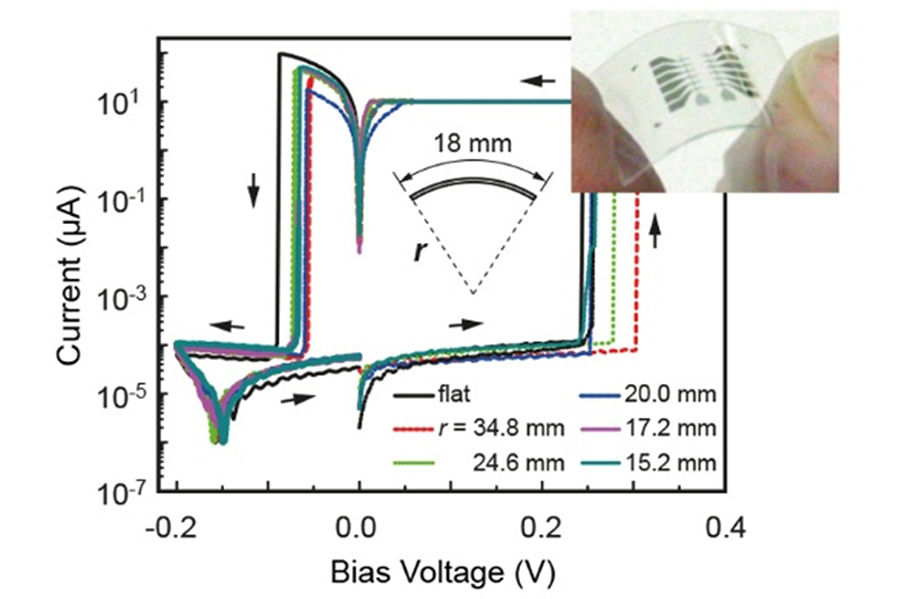
We have demonstrated that atomic switch operation can be realized with organic solid electrolytes. In a MIM structure using a solid polymer electrolyte (SEM), in which several percent of AgCIO4 is dissolved into Polyethylene oxide (PEO), resistive switching arising from the formation and dissolution of a metal filament was observed, similar to oxide-based atomic switches. PEO is well known as a Lithium-ion battery base material. Moreover, utilizing the mechanical flexibility of PEO, we succeeded in fabricating an atomic switch cell on a plastic substrate using an SPE film coated by ink-jet printing, and found that the cell exhibited stable switching characteristics under substrate bending, as shown in Figure 10. This result indicates that the polymer-based atomic switch has potential for use in flexible electronics applications.
2.6 Synapse device based on the atomic switch
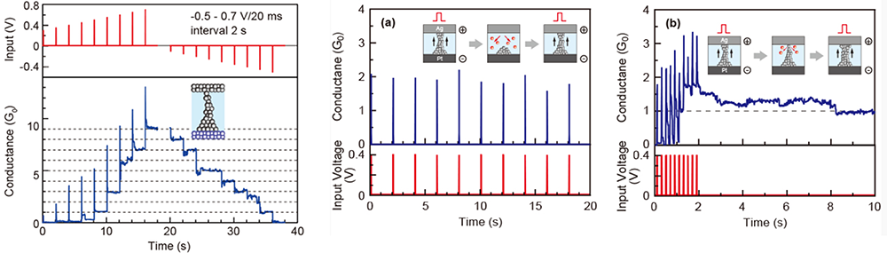
With the rapid advancement of AI in recent years, there is a growing demand for next-generation AI hardware that operates with low power consumption. We are developing neuromorphic devices that possess advanced information processing capabilities while consuming low power (~20 W), corresponding to that of biological brain. Artificial synapse devices are one of the prime examples of the neuromorphic devices, capable of expressing the plasticity observed in neural networks in response to external stimuli. For instance, Ag/Ta₂O₅/Pt and Ag/PEO/Pt junction atomic switches exhibit the unique properties (i.e., quantized conductance and synaptic behavior) by utilizing the formation and dissolution of metal filaments. Figure 11(left) shows the conductance response when positive voltage pulses (0.3 – 0.7V, 20 ms width) are applied successively to an Ag/Ta2O5/Pt cell. By controlling the duration and amplitude of the voltage pulses, it is possible to increase the cell conductance in a stepwise manner. After that, if negative voltage pulses are applied, the cell conductance decreases in a stepwise manner and returns to the original off state. This behavior can be observed repeatedly.
Cell conductance changes significantly when the interval times of the input voltage pulses are varied. Figure 11 (a) (b) represents the variation in cell conductance when voltage pulses are applied with different interval times. For long interval times, the cell conductance returns to zero immediately after the input pulses. In contrast, if voltage pulses are applied with short interval times, the cell conductance gradually increases with accompanying temporary increases and reaches integer multiples of G0 (conductance of a single atomic point contact). These conductance states are maintained for a certain time after the final pulse. This conductance behavior is analogous to the long-term potentiation of biological synapses, in which the strength of the synaptic weight (or conductance) depends upon the time interval between stimulating pulses. In order to achieve this synaptic behavior, at least ten transistors and software preprogramming are required. Since the atomic switch can emulate this function with a single cell, without any software programming, it has the potential for use as a building block for the next generation of neural network systems.
We demonstrated that such operation is also possible in transistor structures. By controlling the magnitude of the applied gate voltage, volatile operation (1.5 V) or non-volatile operation (3.0 V) can be selectively realized (Figure 12). This is attributed to the formation and dissolution of Cu nucleus between the source and drain electrodes, with the structural stability of the Cu nucleus determining whether volatile or non-volatile operation occurs.
3.All-solid-state ion-gate transistor
As shown in Figures 1(c, d and e), we fabricated a three-terminal ion-gate transistor. In this device, applying a gate voltage enables ions to be moved, utilizing the properties of the channel layer (the functional material) to enable operation. We have also demonstrated that solid-state ionic devices made using this method can have various functions.
3.1 All-solid-state electric double layer transistor and all-soli-state redox transistor
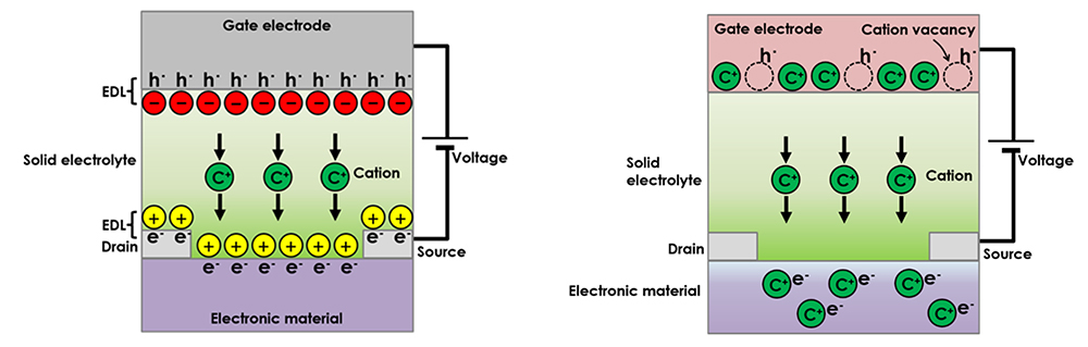
We have demonstrated that solid-state ionic devices possess various functionalities. In the all-solid-state electric double layer transistor, illustrated in Figure 13 (left), ion transport occurs inside a solid electrolyte layer, accompanied by the piling up of ions near the solid electrolyte/electronic material interface. An electronic carrier, with an opposite charge polarity, is accumulated in the vicinity of the interface due to charge compensation. That is to say, the electric double layer consists of high-density ions and electronic carriers that face each other. The electronic carrier density can be reversibly controlled by the electric double layer because the charge density of the electric double layer depends on an external electric field (gate voltage). A significant advantage of the electric double layer is its huge capacitance (> several tenths µF/cm2), which leads to high density electronic carrier doping despite the fact that the electric double layer transistor is an electrostatic carrier doping method, which usually exhibits small capacitance. The technique is particularly advantageous for application to electronic materials in which the physical properties of the electronic structures are sensitive to disturbance caused by chemical doping or non-stoichiometry (e.g. superconductivity).
When a gate voltage is applied to the all-solid-state redox transistor shown in Figure 13 (right), While ion transport occurs within the solid electrolyte, similar to an electric double-layer transistor, ions are also inserted in an electronic material. The electronic carrier is doped in the electronic material by charge compensation. The technique used for electronic carrier control is a redox transistor. Compared to conventional semiconductor technology, the advantage of this technique is that nonvolatile operation can be achieved with a redox mechanism, including relatively slow process times.
3.2 Manipulation of physical properties via the Electric double layer effect
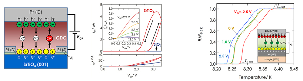
The electric double layer effect can manipulate electrical resistance, superconduction transition temperature, and so on. Superconductivity holds the potential to solve serious environmental and energy problems facing modern society. It is also an important technology expected to be applied to superconducting computers in the information and communications field, which feature ultra-high speed and low power consumption. Raising the superconducting transition temperature, especially achieving room-temperature superconductivity, is the ultimate goal in solid physics. We are exploring high temperature superconductivity with high density electronic carrier doping in potential high temperature superconductors, using all-solid-state electric double layer transistors as the foundation. Candidate solid electrolytes include oxide ion conductors and lithium-ion (Li+) conductors. We demonstrated that an all-solid-state electric double-layer transistor combined with the insulator SrTiO3 can significantly modulate the small current flowing through SrTiO3—less than nA-to a much larger current of μA. Furthermore, we fabricated an all-solid-state electric double-layer transistor combining a lithium-ion conductor with the well-known metallic superconductor Nb and succeeded in modulating the superconducting transition temperature (Figure 14).
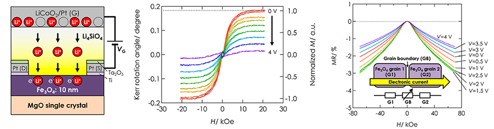
3.3 Magnetic property control using redox reactions
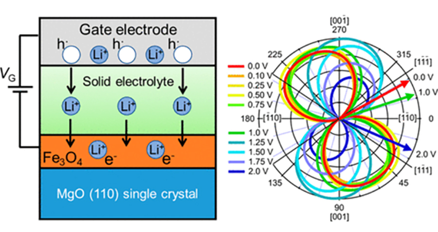
High-density magnetic storage devices (e.g. hard disks, magneto-optical disks, and MRAM) have become even more important due to the information explosion now underway. Since these devices operate on the basis of the tuning of magnetic properties, including magnetization, magnetoresistance (MR), and Kerr rotation angle, development of a technique for property tuning in thin film devices should lead to the generation of technological innovations in high-density storage, low power consumption, high operating speed, and so on. We have developed all-solid-state redox devices composed of ferromagnetic Fe3O4 thin film, which is a promising material due to its half metallicity (Figure 15 left). Figures 15 (middle) and (right) show magnetization and the MR effect tuned by DC voltage application. Magnetization and MR were reversibly tuned by modulation of the spin number in the Fe3O4 due to the insertion and removal of lithium ions. Furthermore, by controlling the crystal growth orientation of the Fe₃O₄ thin film, we found that the magnetization direction also changes, as shown in Figure 15 (below), achieving a magnetization rotation of 56°at room temperature. This result is expected to be applicable not only as a low-power, switchable memory device that does not require an external magnetic field but also for neuromorphic devices utilizing the complex dynamics between ions and magnetization.
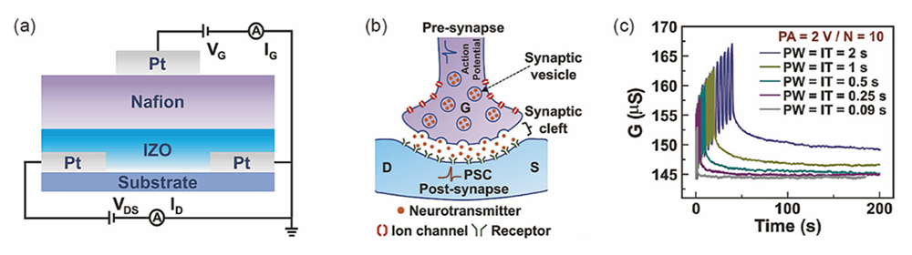
3.4 All-Solid-State Redox Synapse Transistor
For an all-solid-state redox transistor exhibiting synaptic behavior, we have fabricated an all-solid-state redox synapse transistor using an oxide composed of In and Zn (IZO) as the channel combined with the proton conductor Nafion and demonstrated its operation (Figure 17 (left), (middle)). Applying a pulsed gate voltage enables control of the channel conductance by utilizing proton insertion/extraction (i.e., reduction/oxidation) between the IZO channel and Nafion. Applying a pulse voltage increases the channel conductance of the IZO channel. The device exhibited short-term memory for shorter pulse widths, wherein the channel conductance decayed back to the initial state. As the pulse width became longer, the channel conductance decreased initially but maintained a constant level for for a certain period, which is analogous to a long-term memory, after final pulse input (Figure 17 (right)). The short-term memory behavior is mainly determined by proton diffusion within the IZO channel, while the long-term memory state is dominated by proton diffusion in the Nafion.
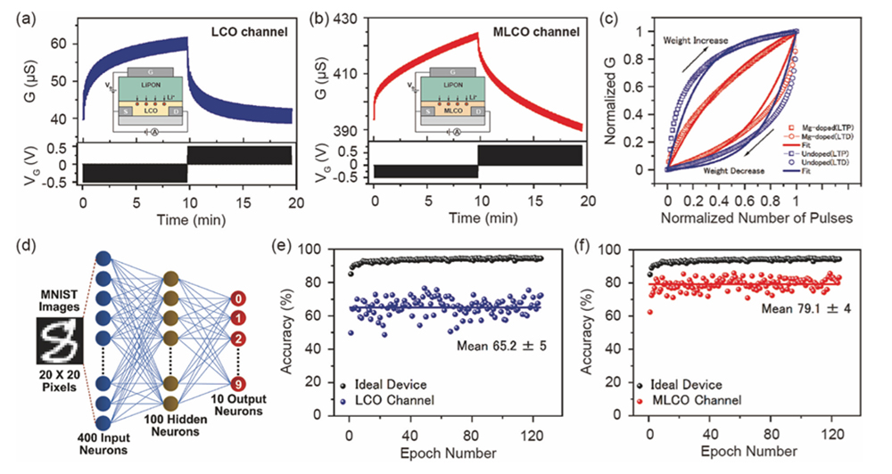
Transistors utilizing lithium solid electrolytes are also promising materials for realizing hardware neural networks for analog computing and are being studied with various combination of lithium electrolytes and channel materials. Among these, LiCoO2 is a promising material as an electrode for lithium-ion batteries and is used as the channel in synapse transistors. We succeeded in significantly suppressing the nonlinearity observed in LiCoO₂ by partially substituting Mg²⁺ for Co³⁺ sites in LiCoO₂, thereby greatly reducing the nonlinearity in the electrical conductivity response to pulse inputs (Figures 18(a)-(c)). Utilizing this, we evaluated the accuracy rate for handwritten character recognition in a fully connected neural network comprising input, hidden, and output layers, as shown in Figure 18 (d). Compared to the 65% accuracy rate of LiCoO₂-based transistors (Figure 18(e)), Mg²⁺-substituted LiCoO₂-based transistors achieved a 79% accuracy rate (Figure 18(f)). This not only resulted in a significant improvement in computational performance but also reduced epoch-to-epoch variability, enhancing reliability. This study demonstrates that element substitution in all-solid-state redox synapse transistors is highly effective for improving the performance of neuromorphic systems.
4.Capacitive devices
We are developing compact, high-capacity electrochemical capacitors that utilize electric double layers and the electrochemical reactions generated by ion transport within solid electrolytes.
4.1 Electrochemical capacitor
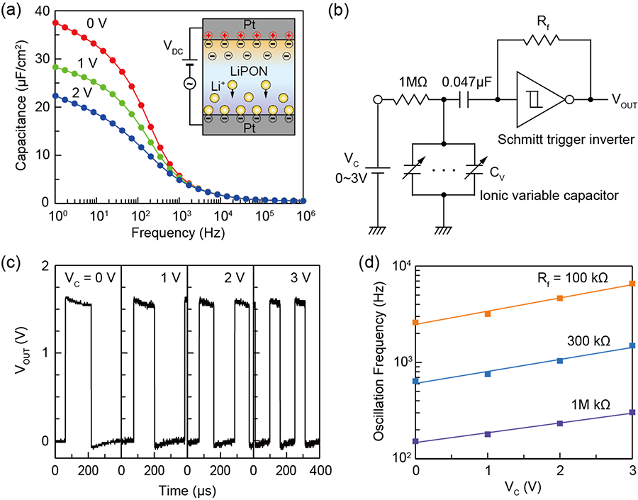
Variable capacitance functions are demonstrated utilizing the transport of Li ions in a simple Pt/lithium phosphorous oxynitride (LiPON)/Pt structure (Figure 19). The capacitance originates mainly from the formation of an electrochemical double layer (EDL) at the interfaces between LiPON and Pt at lower frequencies. Voltage applications drive Li ions from the positively-biased electrode to the negatively-biased one. At higher voltages, the number of Li ions at the positive electrode decreases to zero, which makes their contribution to the total EDL capacitance vanish. As a result, the LiPON capacitor exhibits decreased capacitance as voltage bias is increased, similar to what is found in a varactor diode. The upper frequency limit of the capacitance variation increases with increased temperature, which seems to be determined by the ionic conductivity of the LiPON matrix. A voltage-controlled oscillator (VCO) operation is also demonstrated by incorporating the LiPON variable capacitors into a resistor-capacitor (RC) oscillator circuit. The VCO clearly shows that the oscillation frequency of the output waveforms is exponentially increased by an increase in input direct-current voltage, which behavior is the same as a varactor diode-based VCO. The results indicate that this ionic capacitor can be used as a building block in analog and mixed signal electronic circuits.
5.Visual devices
We are developing visual sensors that enable compact, low-power edge image detection. These sensors leverage hardware rather than relying on software-centric edge image detection, as was the case in the past.
5.1 Visual ionic devices
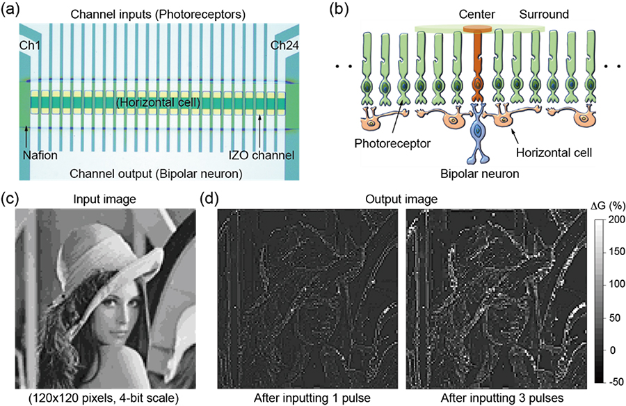
Lateral inhibition is a phenomenon observed in retinal neurons that enhances edge perception and increases the contrast of visual images. To demonstrate lateral inhibition by hardware, our group has proposed a Li ion migration-driven multi-channel device in which one-dimensional (1D) lithium cobalt oxide (LCO) channels are arranged on a lithium phosphorus oxynitride (LiPON) electrolyte (Figure 20). Since Li ions migrate between LCO channels through a common LiPON electrolyte under voltage pulse applications, the device exhibited excitation/inhibition behavior between neighboring channels. Using this characteristic, the edge detection of visual images was simulated by assuming a 2D channel array structure. We also develop a novel proton migration-driven multi-channel device, which is designed for edge detection in real images by employing the principle of lateral inhibition. The device comprises 24 indium zinc oxide (IZO) channels interconnected via proton migration within a common Nafion electrolyte, enabling high interactivity among the IZO channels. The conductance of the respective channels is determined by the proton concentration in the channels as a result of intercalation and de-intercalation of protons with voltage pulse applications. The device clearly mimics various retinal functions, such as center-surround antagonism and optical illusions such as the Mach band and Hermann grid, in which perceived contrast is enhanced at the edges between dark and bright areas. Based on these characteristics, we used the multi-channel device to extract the edge information from real images by utilizing the intrinsic properties of the ionic materials. These results suggest that proton-based highly interactive devices have the potential in use for applications related to the development of artificial hardware-oriented vision systems.
6.Molecular junction switches
We are developing a switch that operates at the single-molecule level, based on the metal filament of an atomic switch.
6.1 Molecular junction switch utilizing Atomic Switch
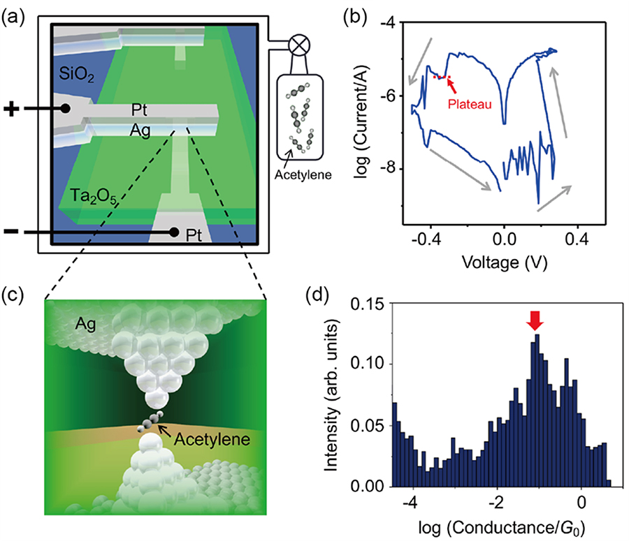
Molecular electronics is attracting increasing attention due to its potential application in post-silicon electronics. However, fabrication of molecular junctions, the fundamental building block of molecular electronic devices, requires complicated procedures, which hamper the efficient development of novel devices. We have proposed a simple fabrication process by utilizing an atomic switch operated by redox reaction and migration of metal atoms (Figure 21). A Ag/Ta2O5/Pt atomic switch is placed in a vacuum chamber, in which acetylene molecules are introduced through a capillary. The typical current-voltage (I-V) curve measured in the acetylene atmosphere exhibits a current plateau after the RESET process. The constant current characteristic during the breakdown of atomically thin metal wires has been commonly observed in mechanical break-junctions and is indicative of the formation of a metastable structure. As this metastable structure, the most likely possibility is the accommodation of an acetylene molecule within the gap of the silver filament. Conductance histogram constructed from I-V curves shows a broad state around 10-1 G0, whose conductance is lower than that of a single atomic contact. Inelastic electron tunneling spectroscopy and first-principles calculations revealed that the observed conductance state is attributed to an acetylene molecular junction formed between Ag filaments. The proposed method can pave the way for the development of single molecular devices based on atomic switch technology, enabling the integration of different molecular junctions and/or atomic switches.
7.Atomic layer deposition (ALD) method.
The ALD is an advanced technology capable of creating extremely thin films at the atomic level. It is expected to play a crucial role in the construction of nanodevices. We are using the ALD to develop a variety of nanodevices.
7.1 Fabrication of solid electrolyte membranes using ALD
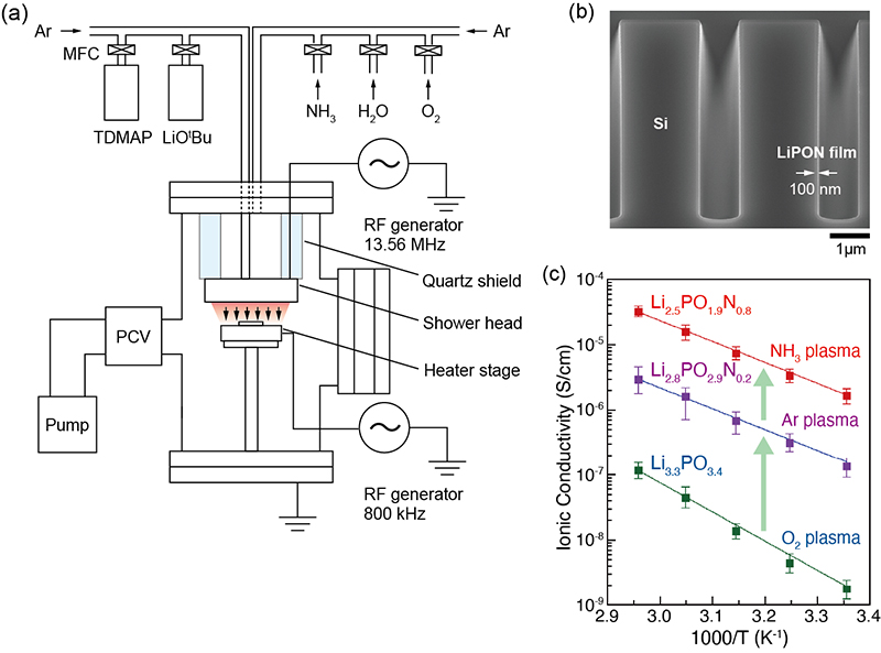
Thin ion conductor films are very important components of ion batteries and fuel cells as well as essential parts of nanoionic and information technology devices. Radio-frequency sputtering and pulsed laser deposition are used to produce solid electrolyte films. However, it is difficult to use these techniques to deposit uniform thin films on three-dimensional (3D) microbatteries and integrated circuits. Recently, the ALD has attracted attention as a technique that can fabricate uniform solid electrolyte films with no pinholes on complex structures with atomic-level precision. We have investigated the effects of plasma reactants on the plasma-assisted ALD of lithium phosphate in relation to the fabrication of high-quality lithium phosphorus oxynitride (LiPON) thin films for the potential use as a solid-state electrolyte (SSE) in both microbatteries and neuromorphic devices (Figure 22). Our ALD processes enable the incorporation of nitrogen into a lithium phosphate matrix, using lithium tert-butoxide (LiOtBu) and tris(dimethylamino)phosphine (TDMAP) as the lithium and phosphorus precursors, respectively, in a deposition temperature window of 220-300 °C. With O2 plasma, polycrystalline lithium phosphate films, with a relatively well-arranged pyrophosphate, are deposited. Amorphous LiPON films, with a mixture of pyrophosphates and orthophosphate, are obtained when Ar or NH3 plasma is used. When the NH3 flow rate increases, the nitrogen composition increases up to ~13%, while residual carbon is kept to below a few percent. For a Li2.5PO1.9N0.8 film deposited at 300 °C with NH3 plasma, the ionic conductivity is measured as 1.65 ± 0.42 × 10⁻⁶ S/cm at 25 °C, with an activation energy of 0.66 eV. This conductivity is the highest value of any ALD LiPON film reported to date. Our ALD processes exhibit a high level of controllability of the molecular structures of the phosphorus oxynitride matrix, with high ionic conductivity, which makes them suitable for realizing high-performance Li SSE thin films.
Reference