Some of major facilities for micro structure analyses are shown here. For further information, please see the following webpage.
Major Facilities of Research Center for Magnetic and Spintronic Materials (CMSM)
The 3D atom probe method can detect and identify the position of single atoms including light elements, which are difficult to observe with electron microscopes. It is also very effective in analyzing the distribution of elements within a variety of materials or devices including semiconductors and ceramics.
In addition, the development of the microfabrication method using FIB technique makes site specific atomprobe specimen preparation possible, such as grain boundaries, specific region of devices.
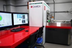
(Left: Local Electrode Atom Probe LEAP5000XS, Right: Laser Assisted Wide Angle 3D Atom Probe developed by NIMS)
What's 3DAP?
Some examples of 3DAP analysis (go to NIMS-CAMECA 3DAP Lab. website)
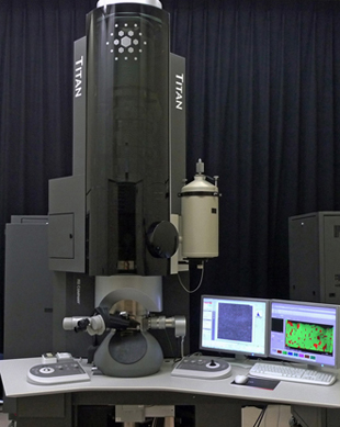
(FEI Titan G2 80-200)
In the system, SEM observation, preparation of TEM and 3DAP samples by standard lift-out method are possible. In addition, it supports EDS(Energy Dispersive x-ray Spectroscopy) and EBSD(Electron BackScatter Diffraction) analysis.
(Left: DualBeam Helios5UX (ThermoFisher), Right: CrossBeam550laser (CarlZeiss))
In the FEI DualBeam Helios5UX, Preparation of TEM/3DAP samples at low temperature(~around 100K) is available in the machine. In addition, it supports automated FIB fabrication and SEM observation by using Python-based API. Also, transferring 3DAP samples between FIB-SEM and 3DAP machine kept at low temperature and without air exposure is possible by using VCTM(Vacuum and Cryo Transfer Module).
On the other hand, Large ROI can be milled by the femtosecond laser in CarlZeiss CrossBeam550laser.
Three-dimensional Atom Probe
The 3D atom probe method can detect and identify the position of single atoms including light elements, which are difficult to observe with electron microscopes. It is also very effective in analyzing the distribution of elements within a variety of materials or devices including semiconductors and ceramics.
In addition, the development of the microfabrication method using FIB technique makes site specific atomprobe specimen preparation possible, such as grain boundaries, specific region of devices.
(Left: Local Electrode Atom Probe LEAP5000XS, Right: Laser Assisted Wide Angle 3D Atom Probe developed by NIMS)
STEM; Scanning Transmission Electron Microscope
(FEI Titan G2 80-200)
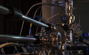
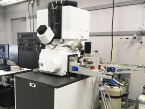
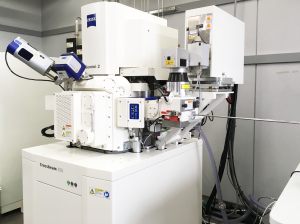
FIB(Focused Ion Beam) and SEM(Scanning Electron Microscope) combined System
In the system, SEM observation, preparation of TEM and 3DAP samples by standard lift-out method are possible. In addition, it supports EDS(Energy Dispersive x-ray Spectroscopy) and EBSD(Electron BackScatter Diffraction) analysis.
(Left: DualBeam Helios5UX (ThermoFisher), Right: CrossBeam550laser (CarlZeiss))
In the FEI DualBeam Helios5UX, Preparation of TEM/3DAP samples at low temperature(~around 100K) is available in the machine. In addition, it supports automated FIB fabrication and SEM observation by using Python-based API. Also, transferring 3DAP samples between FIB-SEM and 3DAP machine kept at low temperature and without air exposure is possible by using VCTM(Vacuum and Cryo Transfer Module).
On the other hand, Large ROI can be milled by the femtosecond laser in CarlZeiss CrossBeam550laser.