 Press Release 2022
Miniaturization of a Thermoelectric Device Capable of Powering IoT Products
—Semiconductor Microfabrication Technology Enables Voltage Output Greater than 0.5 V—
National Institute of Advanced Industrial Science and Technology (AIST)
University of Tsukuba
Using a semiconductor microfabrication technology, a research team consisting of NIMS, AIST and the University of Tsukuba has succeeded in developing a thermoelectric device consisting of an array of π junctions, each composed of two types of thermoelectric layers connected by a metal electrode layer.
“Miniaturized in-plane π-type thermoelectric device composed of a II–IV semiconductor thin film prepared by microfabrication”
Isao Ohkubo, Masayuki Murata, Mariana S. L. Lima, Takeaki Sakurai, Yuko Sugai, Akihiko Ohi, Takashi Aizawa, Takao Mori;
Journal: Materials Today Energy [June 18, 2022];
DOI : 10.1016/j.mtener.2022.101075
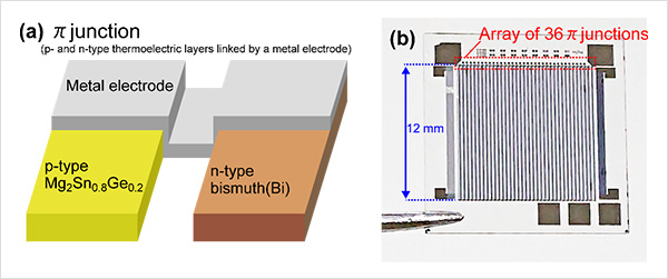
Figure. (a) Enlarged view of a π junction composed of two types of thermoelectric layers connected by a metal electrode. (b) Photo of the thermoelectric device consisting of an array of π junctions.
Abstract
Thermoelectric conversion modules designed to IoT and other electronic devices need to be integrated into these devices. Most previously developed versions of these modules were made of bulk materials, which are incompatible with miniaturization and integration. The output voltages of thermoelectric conversion modules and devices generally decrease as their sizes diminish. An approach to overcoming this miniaturization-related issue is to create an array of π junctions in a thermoelectric device. This research team created a thermoelectric device using a semiconductor microfabrication technology which can be used to produce micro-scale π junctions with a high degree of precision.
This research team fabricated an in-plane thermoelectric device consisting of a dense array of π junctions, each composed of a p-type Mg2Sn0.8Ge0.2 thin film with high thermoelectric generation efficiency and low electrical resistance, an n-type bismuth layer, which can be produced at room temperature. Despite its small size, this device, equipped with an array of 36 tiny π junctions, was able to generate voltages greater than 0.5 V, satisfying a criterion for certain IoT device operations.
The technique used in this research to create smaller, more compact thermoelectric devices may be used to develop new IoT and other electronic products integrated with thermoelectric devices.
This research was supported by the JST-Mirai project entitled "Utilizing magnetism to develop high-performance thermoelectric materials and devices” (project leader: Takao Mori, project number: JPMJMI19A1).
This research was published in Materials Today Energy, an online journal, on June 18, 2022 (URL: https://doi.org/10.1016/j.mtener.2022.101075). A photo from this publication was used in the figure above with some modifications.
(Regarding this research)
Isao Ohkubo
Principal Researcher
Thermal Energy Materials Group, Nano-materials Field, MANA, NIMS
Tel: +81-29-860-4761
E-Mail: OHKUBO.Isao=nims.go.jp
(Please change "=" to "@")
(General information)
Public Relations Office
National Institute for Materials Science
Tel: +81-29-859-2026
Fax: +81-29-859-2017
E-Mail: pressrelease=ml.nims.go.jp
(Please change "=" to "@")
Media Relations Office
Public Relations Department
National Institute of Advanced Industrial Science and Technology
AIST Tsukuba Central 1, 1-1-1 Umezono, Tsukuba, Ibaraki 305-8560, Japan
Tel: +81-29-862-6216
E-Mail: hodo-ml=aist.go.jp
(Please change "=" to "@")
Bureau of Public Relations
University of Tsukuba
1-1-1 Tennodai, Tsukuba, Ibaraki 305-8577, Japan
Tel: +81-29-853-2040
Fax: +81-29-853-2014
E-Mail: kohositu=un.tsukuba.ac.jp
(Please change "=" to "@")