 Press Release 2021
Development of a High-Energy-Resolution, LaB₆ Nanowire-Based Field Emission Gun
—Electron Source Enables Atomic Resolution TEM Observation—
JEOL Ltd.
The National Institute for Materials Science (NIMS) and JEOL, Ltd. have developed a lanthanum hexaboride (LaB₆) nanowire-based field emission gun that is installable on an aberration-corrected transmission electron microscope (TEM).
“High-endurance Micro-engineered LaB₆ Nanowire Electron Source for High-resolution Electron Microscopy”
Han Zhang, Yu Jimbo, Akira Niwata, Akihiro Ikeda, Akira Yasuhara, Cretu Ovidiu, Koji Kimoto, Takeshi Kasaya, Hideki T. Miyazaki, Naohito Tsujii, Hongxin Wang, Yasushi Yamauchi, Daisuke Fujita, Shin-ichi Kitamura, Hironobu Manabe;
Journal: Nature Nanotechnology [November 9, 2021, Japan Time];
DOI : 10.1038/s41565-021-00999-w
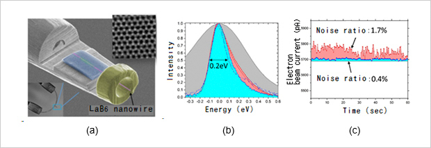
Figure. (a) SEM image of the LaB₆ nanowire-based electron source. An atomic resolution image of single-layer graphene taken by a TEM equipped with this electron source is shown in the boxed image at upper right.
(b) Comparison of the electron beam energy distributions of the LaB₆ nanowire-based electron source (blue), the conventional tungsten field emission electron source (red) and the conventional Schottky electron source (gray).
(c) Comparison of the noise ratios of the LaB₆ nanowire-based electron source (blue) and the conventional tungsten field emission electron source (red).
Abstract
Unsuccessful efforts have been made for more than 20 years to develop field emission guns using theoretically high-performance nano materials. It has been found challenging to integrate a nanowire-based field emission gun into an electron microscope without undermining its physical properties, such as lives and stability. For this reason, commercially available field emission guns are still equipped with tungsten needles developed more than half a century ago.
This NIMS-JEOL research team 1) developed techniques to chemically synthesize and grow high-purity, single-crystal nanowires of LaB₆, known to be an excellent electron-emitting hot cathode material, 2) designed an electron source mechanism capable of efficiently emitting electrons and 3) developed techniques to extract a single nanowire and integrate it into an optimized electron source structure.
The LaB₆ nanowire-based electron source has a number of advantages: relatively moderate vacuum condition requirements, very high current stability, low extraction voltage, narrow electron beam energy distribution width and high brightness. This electron source may be applicable to the development of next-generation field emission electron microscopes with higher spatial and energy resolution—potentially valuable tools in the semiconductor and medical fields.
This project was carried out by a team of NIMS researchers (Han Zhang, Cretu Ovidiu, Koji Kimoto, Takeshi Kasaya, Hideki T. Miyazaki, Naohito Tsujii, Hongxin Wang, Yasushi Yamauchi and Daisuke Fujita) and JEOL researchers (Yu Jimbo, Akira Niwata, Akihiro Ikeda, Akira Yasuhara, Shin-ichi Kitamura and Hironobu Manabe).
This research was published in the online version of Nature Nanotechnology on November 9, 2021, Japan Time (DOI: 10.1038/s41565-021-00999-w).
(Regarding this research)
Koji Kimoto
Director
Research Center for Advanced Measurement and Characterization
National Institute for Materials Science
Tel: +81-29-860-4402
E-Mail: KIMOTO.Koji=nims.go.jp
(Please change "=" to "@")
Zhang Han
Senior Researcher
Electron Microscopy Group
Research Center for Advanced Measurement and Characterization
National Institute for Materials Science
E-Mail: Zhang.han=nims.go.jp
(Please change "=" to "@")
(General information)
Public Relations Office
National Institute for Materials Science
Tel: +81-29-859-2026
Fax: +81-29-859-2017
E-Mail: pressrelease=ml.nims.go.jp
(Please change "=" to "@")
JEOL Ltd.
Corporate Communication Department
Management Strategy Planning Division
3-1-2 Musashino, Akishima, Tokyo 196-8558, Japan
Tel: +81-42-542-2106
Fax: +81-42-546-9732
E-Mail: ir=jeol.co.jp
(Please change "=" to "@")