 Press Release 2018
Development of a Multi-Value Logic Circuit Composed of Organic Transistors
—New Technology May Increase the Performance of Flexible Electronics—
By combining two types of organic transistors, the National Institute for Materials Science (NIMS) has succeeded in developing a multi-value logic circuit capable of switching between three values.
(“Multi-valued logic circuit based on organic anti-ambipolar transistor” Kazuyoshi Kobashi,Ryoma Hayakawa Toyohiro Chikyow, Yutaka Wakayama Nano Letters 2 July 2018; doi:10.1021/acs.nanolett.8b01357)
Electronic devices composed of light and flexible organic materials are highly portable and can be processed into large-area electronics using specialized printing techniques. Because of these advantages, these materials have been used in the development of wearable devices capable of monitoring perspiration and heart rate. In addition, significant improvements in the properties of organic transistors have been pursued as a way of increasing the data processing capabilities and communication speeds required for widespread use of IoT technology. However, miniaturization and high-density integration techniques are inapplicable to devices based on organic materials because they are incompatible with the microfabrication techniques developed in semiconductor device R&D, necessitating the development of novel techniques to increase performance.
To address this issue, the NIMS research group developed a device composed of a combination of a unique transistor (an anti-ambipolar transistor [AAT], in which the current drain decreases when the gate voltage increases above a certain level) and an ordinary transistor (see the diagram on the left in the figure below). When the device’s gate voltage is low, a stronger electric current flows through the AAT than through the ordinary transistor. As the gate voltage increases, electric current flows at similar rates between the two transistors. As the gate voltage increases further beyond a certain level, the electric current traveling through the AAT decreases, resulting in a stronger electric current passing through the ordinary transistor.
The unique device structure we developed by combining two types of transistors with different electric current characteristics is able to switch between three values. This technology potentially enables the development of logic circuits capable of controlling multiple output values. The levels of integration and data processing capabilities of transistors can be significantly increased using this technology without increasing their size. In future studies, we hope to achieve the high-density integration of organic materials that has proven so difficult and develop new, flexible organic transistors with superior data processing capabilities.
This project was carried out by a research team led by Yutaka Wakayama (leader of the Quantum Device Engineering Group, International Center for Materials Nanoarchitectonics [MANA], NIMS) and Ryoma Hayakawa (Senior Researcher, Quantum Device Engineering Group, MANA, NIMS). The project was conducted as part of the Grant-in-Aid for Challenging Exploratory Research project entitled “Development of a tunnel transistor with a molecular superlattice.”
This research was published in the online version of Nano Letter, a journal of the American Chemical Society, on July 2, 2018.
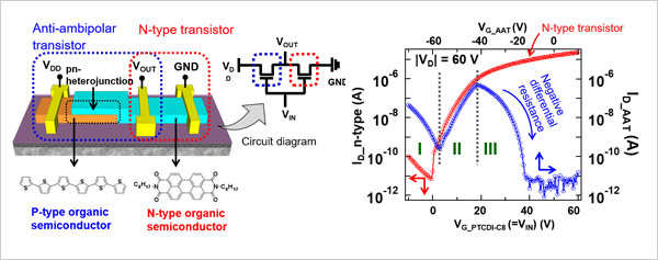
Figure. New organic transistor
(Regarding this research)
Yutaka Wakayama
Deputy Director,
Quantum Device Engineering Group, MANA, NIMS
Tel:+81-29-860-4403
E-Mail:WAKAYAMA.Yutaka=nims.go.jp=nims.go.jp
(Please change "=" to "@")
Ryoma Hayakawa
Senior Researcher,
Quantum Device Engineering Group, MANA, NIMS
Tel:+81-29-860-4808
E-Mail:HAYAKAWA.Ryoma=nims.go.jp=nims.go.jp
(Please change "=" to "@")
(For general inquiries)
Public Relations Office
National Institute for Materials Science
1-2-1 Sengen, Tsukuba, Ibaraki, 305-0047, JAPAN
Tel:+81-29-859-2026
Fax:+81-29-859-2017
E-Mail:pressrelease=ml.nims.go.jp
(Please change "=" to "@")