 Press Release 2017
Development of a Vertical Resonant Tunneling Transistor that Employs Molecules
- Compatible with the Existing Microfabrication Processes, the New Technology May Enable the Development of a Novel Transistor Superior to Silicon Transistors in Performance -
A NIMS research group succeeded in fabricating and demonstrating the operation of a vertical resonant tunneling transistor with molecular quantum dots.
(“Vertical resonant tunneling transistors with molecular quantum dots for large-scale integration”; Ryoma Hayakawa, Toyohiro Chikyow and Yutaka Wakayama; Nanoscale, 2017, 9, 11297-11302, DOI: 10.1039/C7NR02463K)
Molecular devices in which individual molecules serve as transistor and memory elements are believed by many to be ultimate in nanoelectronics. Over the past 20 years, techniques have been developed to measure the electrical conductivity of single molecules, leading to the discovery of useful molecular functions. However, ways of integrating molecular devices remain under development. Research activities have not advanced beyond evaluation of the basic physical properties of molecular devices. Meanwhile, tunnel transistors and single-electron transistors capable of multilevel operations have begun to attract attention due to their potential to be faster, more integration compatible and more energy-efficient than silicon transistors. However, the working principle of a tunnel transistor is no different than that of a conventional transistor; both alternate between two states, allowing only two digits: 0 and 1. In addition, practical use of single-electron transistors is still not on the horizon due to the challenge of fabricating nanoscale quantum dots of uniform size.
To resolve these issues, the research group developed a technique to integrate molecules between two insulators without damaging the molecules. We also demonstrated that resonant tunneling current can flow between two insulators in a transistor in which molecular quantum dots are incorporated. We were able to control the size of the molecules used by synthesizing equally sized nanoscale molecules. In addition, we demonstrated that resonant tunneling current flowing in a two-terminal structure can be controlled using several threshold values. We achieved this by controlling molecular energy levels during the molecular design process and before incorporating the molecules into the transistor.
In this research project, which continued our previous research efforts, we fabricated a vertical resonant tunneling transistor by microfabricating a channel layer within which molecules had been embedded between two insulators using existing lithography techniques used in the microfabrication of silicon-based electronic devices. These techniques cannot be applied to create ordinary molecular devices because they involve the use of organic materials—resists and organic solvents—which damage the molecules. However, they can be applied to the transistor structure we developed because the molecules are protected by insulating layers. In addition, we observed in the fabricated transistor that tunneling current changed in stages in response to gate voltages at low temperature (20 K).
The vertical transistor structure we developed will enable a high degree of integration and reduced power consumption due to the use of tunneling current. Our results indicate that multilevel transistor operations can be achieved by properly designing molecules. These results also suggest that the development of next-generation nanotransistors that would be faster, more integration compatible and more energy-efficient than silicon transistors is feasible.
This study was published in Nanoscale, a journal of the Royal Society of Chemistry, on August 1, 2017, local time (6:00 pm on August 1, Japan Time).
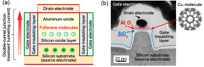
Figure: (a) Schematic of a vertical resonant tunneling transistor within which molecules are embedded. (b) Scanning tunneling electron microscopic image of the cross-section of a fabricated transistor sample. The molecules are individually embedded between an aluminum oxide (Al2O3) layer formed directly under the drain electrode and a silicon oxide (SiO2) layer.
(Regarding this research)
Ryoma Hayakawa
Senior Researcher, Quantum Device Engineering Group, MANA, NIMS
Tel:+81-29-860-4808
E-Mail:HAYAKAWA.Ryoma=nims.go.jp
(Please change "=" to "@")
Yutaka Wakayama
Group Leader, Quantum Device Engineering Group, MANA, NIMS
Tel:+81-29-860-4403
E-Mail:WAKAYAMA.Yutaka=nims.go.jp
(Please change "=" to "@")
(For general inquiries)
Public Relations Office
National Institute for Materials Science
1-2-1 Sengen, Tsukuba, Ibaraki, 305-0047, JAPAN
Tel:+81-29-859-2026
Fax:+81-29-859-2017
E-Mail:pressrelease=ml.nims.go.jp
(Please change "=" to "@")