


3-Dimensional Atomic Tomography of Ceramics
3D atom probe using ultraviolet laser pulses
Jun. 15, 2009
Ultraviolet femtosecond pulse laser
The National Institute for Materials Science and the Japan Science and Technology Agency succeeded in atomic-level 3-dimensional (3D) tomography of a stabilized zirconia-spinel nanocomposite, which is an insulating ceramic. In the analysis, a 3D atom probe operated with ultra-violet (UV) laser pulses was used to identify the positions and elemental species of individual atoms. The work was carried out by the group of Kazuhiro Hono, a Principal Investigator (PI) at the NIMS International Center for Materials Nanoarchitectonics (MANA) and Tadakatsu Ohkubo, Group Leader of the Nanostructure Analysis Group, Magnetic Materials Center at NIMS, in collaboration with Yimeng Chen, a graduate student at the University of Tsukuba.
Using transmission electron microscopy, obtaining morphological 3D tomography is possible with a spatial resolution of approximately several 10 nm. However, the present work has demonstrated that atomic tomography comprising of millions of atoms can be obtained using the UV laser assisted 3D atom probe. Such atomic resolution in 3D tomography and the quantitativeness of the nanoscale analysis is possible only with this technique. It had been considered impossible to apply the 3D atom probe technique to bulk insulating ceramics.
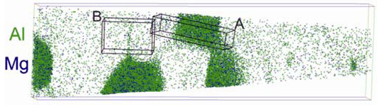
You can see 3D video of 3-dimensional tomography.
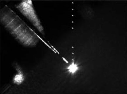
In the atom probe technique, atoms are ionized by applying a high electrical field of 107 V/m to a needle-like specimen. In this research, a needle-like specimen with a tip radius of approximately 50 nm was prepared from a bulk ceramic material using the focused ion beam (FIB) technique, which was then put onto a tungsten needle. A high voltage was applied to the ceramic tip on the tungsten needle, and the tip was irradiated with a femtosecond laser with a wavelength of 330 nm. The ionization of atoms was confirmed to occur in synchronization with the femtosecond laser. Using this laser assisted field evaporation phenomenon, the positions of the individual atoms and their time-of-flights were measured, and 3D atomic tomography was successfully obtained.
In the past, the 3DAP technique has been believed to be applicable to only electrical conductive materials like metals and semiconductors. Unlike the conventional belief, the work has demonstrated that the 3D atom probe technique can be employed to obtain 3D atomic tomography of even insulating ceramics. This work will trigger applications of the 3DAP technique in nanoscale analyses of a wider variety of inorganic materials.

Principle diagram of 3D atom probe tomography
This research was carried out as part of the research topic “Development of Laser Assisted Wide Angle Three-Dimensional Atom Probe and its Applications for Device Analysis” (Research Representative: Kazuhiro Hono) in the research area “Novel Measuring and Analytical Technology Contributions to the Elucidation and Application of Material” (Research Supervisor: Michiyoshi Tanaka, Professor Emeritus, Tohoku University) in the JST’s Core Research for Evolutional Science and Technology (CREST) program team-type research program. The research result was published in the journal Scripta Materialia, 61(7), 693-696, 2009.
National Institute for Materials Science (NIMS)
Japan Science and Technology Agency (JST)
For more information
- Kazuhiro Hono
- Principal Investigator, MANA, NIMS
- Tel: +81-29-859-2718
- E-mail:

- International Center for Materials Nanoarchitectonics (MANA), NIMS
- Tel. +81-29-860-4709
- Fax. +81-29-860-4706
Press Release Success in 3-Dimensional Atomic Tomography of Ceramics on NIMS Website