Research
Our Semiconductor Nano-integration Group is investigating electronic materials, “semiconductors”, which is now indispensable in the modern society. For the NEXT technologies of semiconductor nanomaterials and device integration on the silicon (Si) complimentary metal-oxide-semiconductor field-effect transistor (CMOS) and complimentary field-effect transistor (CFET) platform beyond the “1-nm-process” in 2030s, our Semiconductor Nano-integration Group aims to the research and development of “the Best of Both Worlds”, i.e., top-down and bottom-up approaches, method for the integration of heterogeneous nanomaterials in semiconductor electronics, i.e., the “silicon platform”. Our approach is based on the idea that it is NOT necessary to realize any integration technologies of semiconductor nanomaterials and devices on the silicon platform only by either top-down or bottom-up fabrication methods. The group is going to conduct experiments for the application and creation of semiconductor nanoelectronic devices integrated heterogeneously on the silicon platform, in combination with the fundamental approaches for the fabrication of nanostructures and the characterization of their materials property.
Semiconductor Nanomaterials Integration Technologies by “the Best of Both Worlds”: Top-down and Bottom-up Approaches
The middle-of-line (MOL) and back-end-of-line (BEOL) on the silicon platform need a relatively low growth temperature, e.g., < 400°C, for semiconductor nanomaterials. Based on the original bottom-up fabrication method developed for semiconductor heterogeneous nanomaterials by the group leader and others, our group is investigating and developing the direct site-controlled growth approaches using metal-organic vapor phase epitaxy (MOVPE) and chemical vapor deposition (CVD) for two-dimensional (2D) single crystalline nanosheet channel materials, i.e., 2D transition metal dichalcogenide (TMDC) nanosheets etc., onto the silicon platform, e.g., CFET, in the next generation. The approach in our group presumably enables the semiconductor industry in the world to realize the heterogeneous integration of 2D-TMDC nanosheets site-controlled on the Si nanostructures of CFET by the top-down fabrication methods in Si nanoelectronics.
Integration Technologies for Semiconductor Nanomaterials only Created by Bottom-up Approach
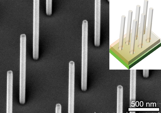
Our novel bottom-up approach, i.e., the site-controlled growth by MOVPE and CVD, enables us to create group III-V compound and group IV semiconductor nanostructures, e.g., vertical free-standing semiconductor nanowires, directly grown heterogeneously on Si wafers, which is not possible to be realized by the conventional top-down fabrication methods for thin-film semiconductors. These nanostructures can be grown at relatively high growth temperature, which is applicable only to the front-end-of-line (FEOL) of Si process and show novel nanoelectronic properties and crystallographic structures, which have not been shown in the bulk and thin films of semiconductors. The aim of our group is to investigate and develop the heterogeneous integration methods on the silicon platform, using the well-established surface activated bonding technology at room temperature, for these novel semiconductor nanomaterials only created by our bottom-up approach. In Figure (a bird’s-eye view taken by scanning electron microscope) below, we formed free-standing vertical InAs nanowire array heterogeneously on the semiconducting substrates, e.g., Si, GaAs, etc., not by the conventional top-down-type etching techniques after the deposition of semiconductor thin films, but by our original bottom-up-type site-controlled crystal growth technique.


