Principle of Atom Probe Tomography
- Field Evaporation & Atom Probe

- Atom Probe Field Ion Microscope (APFIM)
- Principle of Atom Probe Tomography (APT)
Field Evaporation & Atom Probe
Field evaporation is a phenomenon in which atoms are ionized under the presence of extremely high electric fields, typically on the order of a few V/nm. Such intense electric fields can only be achieved by applying a high voltage to a sharply pointed, needle-like specimen. As a result, field evaporation is observed exclusively in Field Ion Microscopy (FIM) or scanning tunneling microscopy (STM). The movie in Fig. 1 shows tungsten atoms field evaporating from the tip apex surface of a tungsten specimen, as observed by FIM. Evaporation (ionization) occurs only when the electric field is much higher than that required for conventional FIM imaging. The atom probe technique measures the time-of-flight of ions field evaporated from the surface of an FIM tip by controlled application of high-frequency voltage pulses.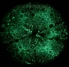
Fig. 1. FIM image (GIF animation) observing field evaporation of tungsten atoms.
Atom Probe Field Ion Microscope (APFIM)
An atom probe field ion microscope (APFIM) combines a field ion microscope (FIM) with a time-of-flight mass spectrometer capable of detecting individual ions. When a high electric field is applied to the surface of a sharp needle tip, imaging gas atoms are ionized at protruding sites on the surface. These ions strike the screen, forming bright imaging spots. FIM is therefore a projection-type microscope with atomic resolution and a magnification of several million times. By applying an even higher electric field, surface atoms of the specimen are also ionized. Through this field evaporation process, atoms are sampled directly from the specimen’s surface. By measuring the time-of-flight of individual atoms that pass through a small aperture at the center of the screen, it is possible to determine the mass-to-charge ratios of each atom. Atoms are collected only within the aperture, whose effective size typically ranges from 0.5 to 5 nm. Thus, the atom probe achieves spatial resolution of this dimension laterally. Because atoms always evaporate from the surface, spatial resolution in the depth direction corresponds to a single atomic layer. A unique feature of the atom probe, compared to other analytical instruments, is its extremely high spatial resolution and equal detection efficiency for light elements.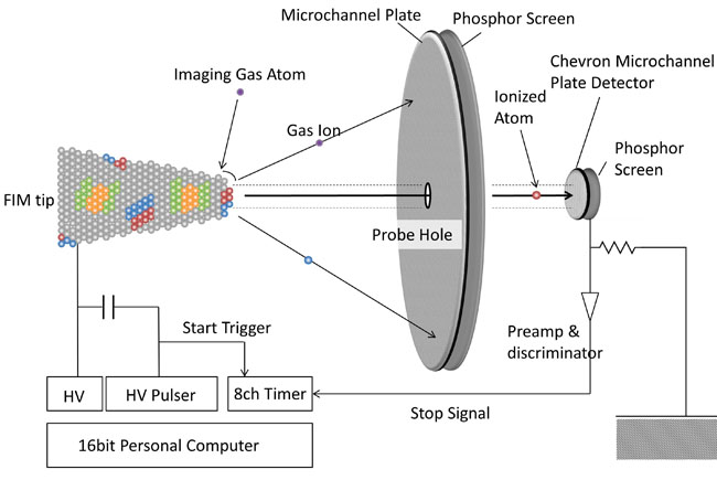
Fig. 2. Principle of Atom Probe Field Ion Microscope (APFIM).
Principle of Atom Probe Tomography (APT)
In 1988, Cerezo, Godfrey, and Smith at the University of Oxford succeeded in determining both the mass-to-charge ratio (m/z) and the position of ions simultaneously by applying a position sensitive detector to a time-of-flight atom probe. They named this novel instrument the position sensitive atom probe (PoSAP), demonstrating that two-dimensional elemental mapping with sub-nanometer spatial resolution was possible. By reconstructing a series of two-dimensional element maps using a graphics workstation, they were able to create three-dimensional element maps within a nanoscale volume. Subsequently, a group at the University of Rouen developed a similar atom probe employing a multiple-anode detector capable of detecting multiple ion arrivals. This instrument was named the tomographic atom probe (TAP), as it could reveal tomographic images of atoms in metallic materials. Both PoSAP and TAP utilize position sensitive detectors, enabling the determination of mass-to-charge ratios and atom positions in conductive materials. This capability allowed observation of atomic distributions in three dimensions at spatial scales of a few tens of nanometers. These techniques are now generally referred to as atom probe tomography (APT).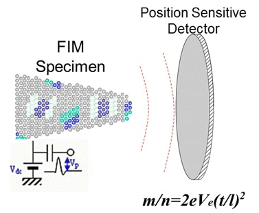
Fig. 3. Principle of APT (GIF animation).
Examples of element and concentration mapping obtained by a PoSAP are shown in Fig. 5. In the element map, individual Fe atoms are represented by red dots, while individual Cr atoms are indicated by blue dots. By counting the number of atoms in each pixel, the element map can be converted into a concentration map, where the concentration for each pixel area of approximately 0.4 × 0.4 nm is displayed using a color scale. The observed area corresponds to about 20 × 20 nm.
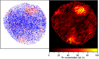
Fig. 4. Element and concentration map of an aged Cr-Fe alloy. Red dots correspond to Fe atoms, and blue dots correspond to Cr atoms.
By sequentially collecting two-dimensional elemental maps as shown in Fig. 4, a three-dimensional atom map can be constructed, as illustrated in Fig. 5. This technique achieves atomic sensitivity as a tomographic method, and the spatial resolution is typically better than 0.2 nm, although this value depends on specimen morphology and variations in evaporation field.
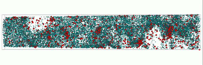
Fig. 5. 3D elemental map (GIF animation) of Nd and Cu atoms in a nanocrystalline Nd-Be-B-Cu alloy. The green and red spheres correspond to Nd and Cu atoms, respectively.