|
 |
|
|

|
|

|
通常の太陽電池では利用できない緑色、青色領域の光を太陽電池に利用できるように実験をしています。 |

|
有機材料と無機材料を組み合わせた新しいデバイスの創出について実験しています。 |

|
パルス熱プラズマから発生する水素ラジカルを利用して高効率にSiが生成できるプロセスについて研究しています。 |

|
サファイア基板上に成長するGaN薄膜、および基板面内での極性構造を制御する方法を紹介しています。 |

|
ZnO薄膜の成長方法とその光学特性について紹介しています。 |
|
|
サファイア基板上GaNテンプレート上のInGaN薄膜成長およびそのp型化について検討して、III-V族太陽電池を作製しています。最近の研究の進展で、InNのバンドギャップが0.65eVと下方修正されたことで、図1のようにInNとGaNとの混晶を形成すれば太陽光スペクトルをほぼ完全にカバーできる点で、次世代の高効率太陽電池材料として期待されています。
InGaN薄膜は2.4eV以上のバンドギャップを持つ、直接遷移型の半導体で、理論的には50%以上の変換効率を実現できます。我々はIn組成の高いInGaN薄膜の成長を検討しながら、構造、光学的電気的特性の向上を行い、p型化およびpn接合形成に関する研究を行っています。フォトリソ、ICPによるエッチング、電子ビーム蒸着などデバイスプロセスをも最適化しながら図2のような太陽電池構造を作製してその特性の向上に努めています。(NEDO革新的太陽電池プロジェクトで)
1.InGaN-based p-n junction solar cells
We study the epitaxial growth of InGaN, p-InGaN films, InGaN-based solar cell structures on GaN/sapphire template and fabricate solar cell devices. As is known, recent discovery on the band gap energy of InN (0.65 eV) makes InGaN a potential candidate for the next-generation solar cells, as its corresponding wavelength nearly covers the whole solar spectrum. InGaN is one of the few material systems that provide direct band gaps greater than 2.4 eV, which are required to achieve practical photovoltaic efficiencies greater than 50%. We focus on the structural, optical and electrical properties analysis on InGaN films with a high In content, p-type doping for InGaN, p-n junction growth optimization, etc. We also focus on the solar cell devices processing using photolithography, ICP, E-beam and RTA, and device properties analysis with regard to electrical and optical measurement.
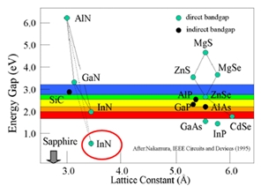
Fig. 1
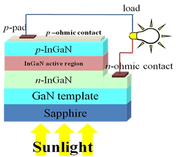
Fig. 2
|
|
|
2.Schottky junction using conducting polymer
In order to study photovoltaic properties of n-GaN and n-InGaN epitaxial layers growth by MOCVD, Schottky device is realized in parallel of p-n junction InGaN study. In general, the Schottky junction is fabricated using metal with higher workfunction like thin gold. For an application to solar cell, an electrode should be transparent. We have used organic polymer of PEDOT:PSS or polyaniline (PANI) as the electrode materials satisfying both high transparency and high conductivity (Fig. 1). Previously studied in our laboratory, Schottky solar cells with TCO polymers reveal good photovoltaic properties (Fig. 2) due to its high work function (5.1eV for PANI and 5.2eV for PEDOT:PSS) and low absorption. To enhance the photovoltaic properties of these devices, it is necessary to improve the Schottky barrier height. Our works focus on interface study and optimization device.
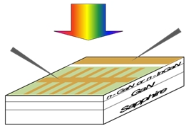
Fig. 1
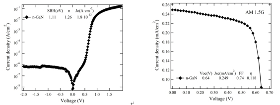
Fig.2 a, b
|
|
|
角谷の実家には6年前から3kWの太陽電池システムを導入している。図1に年ごとの売電量を示す。昨年の売電価格の倍増により平成22年度の半年間で例年の金額を稼いでいて、このままいけば年間10万円を超える電気代を賄うことができる。地球環境・エネルギー問題への危惧から太陽電池を導入する機運が高まっている。CuInGaSeなどの薄膜太陽電池が注目を集めているが、図2に示すNIMS元素戦略の予想では、存在しうるInすべてをCIGS太陽電池に利用したとしてもせいぜい100GWである。真にエネルギーに寄与できる太陽電池材料としてはSi以外にあり得ない状況である。
現在、太陽電池用を含む高純度シリコンは、トリクロロシラン(SiHCl3)と水素ガスとの反応を用いるシーメンス法により工業的に製造されています。この手法では副生成物であるテトラクロロシラン(SiCl4)の生成反応が起こりやすく、最終的なシリコン収率が25%程度と高くないことが課題として上げられています。
これらの課題を解決するために水素ガスに替えて、パルス熱プラズマ(図1)を発生源とした水素ラジカルを用いた研究を進めています。水素ラジカルを用いることで、シーメンス法と同程度の純度を保ちつつ、副生成物の低減、それに伴うシリコン収率の大幅な向上だけでなく、反応の低温化も期待できることが橋本教授(日大)・鯉沼教授(東大)ら熱力学計算によって見出されています。
これまでに、ラマンスペクトル測定から反応室内に導入した基板上に520cm-1の結晶シリコンの存在を示すピークを確認し(図2)、シーメンス法より低温条件でのシリコン生成にも成功しています。将来的には、高収率かつ低コストな太陽電池用シリコンの製造法としての応用を目指しています。
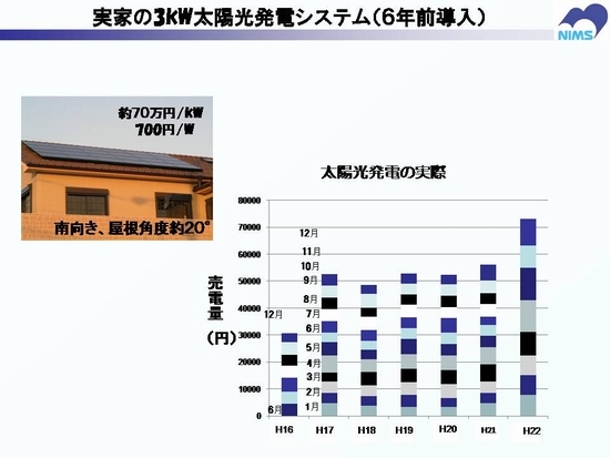
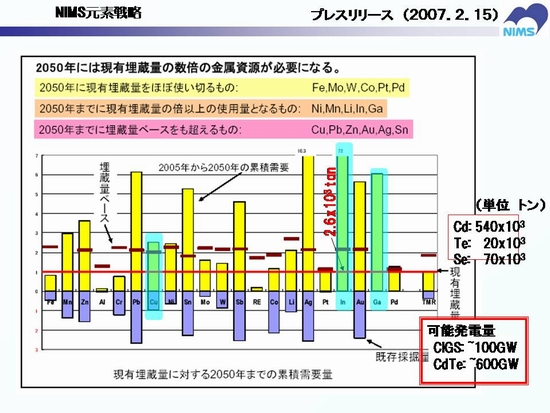
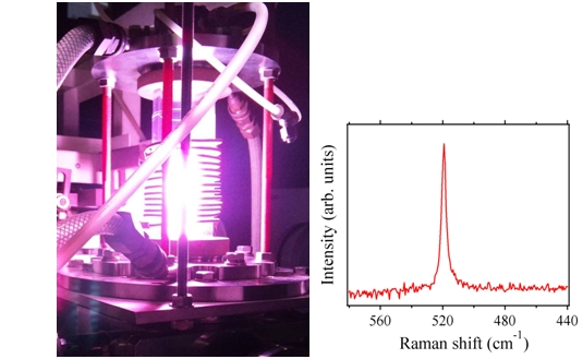
Fig. 1 Fig. 2
Nowadays the majority of solar panels use silicon material because of its mature technology and low price. But, due to the band gap of 1.1eV for crystalline silicon, a large part of solar spectrum is not absorbed (for long wavelengths) or lost by thermalization (for high energetic short wavelengths). Thus, the next generations of solar cells need to have different band gap materials to be more suitable to the solar spectrum and reach high conversion efficiency. |
|
|
サファイア基板上に成長するGaN薄膜、および基板面内での極性構造を制御する方法を紹介しています。
|
 |
|
|
ZnO薄膜の成長方法とその光学特性について紹介しています。
|
|
|
|
|
|
|
|
|
|
|
|
|
|
|
|
|
|
|
 |
|
|
 |
|