|
 |
|
|
|
|
Facilities, short presentation
Our laboratory disposes of equipments for the growth and the characterization of III-V nitride thin film, optical and electronics properties, metal deposition as well as equipments necessary for solar cells characterizations:
|
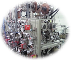
1. Metal Organic Chemical Vapor Deposition (MOCVD) with a horizontal reactor
 |
|
For III-V nitride thin films growth, TriMethylGallium (TMG), TriMethylIndium (TMI), TriMethylAluminium (TMA) and Ammonia (NH3) are used as Ga, In, Al and N sources. It is possible to grow epitaxial thin film on different substrate sizes from 0.5cm2 to 2 inches wafer. |
|
|
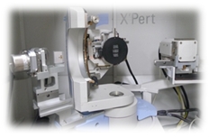
2. X-ray Diffraction (XRD) characterization
 |
|
After optimizing σ,ω,φ and ψ angles, X’Pert Pro equipment is used for 2σ-ω
scan and reciprocal space mappings (RSMs) with a high resolution about
1?10-4 degree. |
|
|
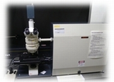
3. Transmittance measurement
|
|
An UV-3150 Shimadzu (large spectral scale from 200nm to 3200nm) is used
to measure the transmittance spectrum of grown thin films and estimate
the optical band gap. |
|
|
4. Photoluminescence (PL) measurement
 |
|
Photoluminescence spectrum can be measured by a couple Cd-He laser + monochromator
in order to determine the optical band ga.
|
|
|
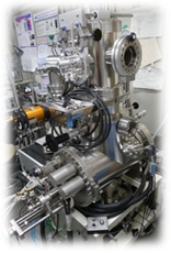
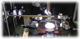
. 5. E-beam evaporator
 |
|
This e-beam evaporator disposes of 3 metallic sources, titanium, gold and
nickel used for ohmic or Schottky contacts. Thicknesses deposited can be
precisely controlled at the scale of 10 nanometers under low vacuum level
about 1~2?10-7 Torr. |
|
|
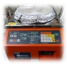
6. Transparent Conductive Organic (TCO) polymer deposition
 |
|
The TCO polymer is deposited by Mikasa spincoater MS-A100 to control efficiently the homogeneity and the films thickness. |
|
|
7. Current-Voltage, Capacitance-Voltage characterization
 |
|
Filtered Xe lamp is used to obtain the standard AM1.5G solar spectrum. The current-voltage (I-V) is precisely measured using Keithley 2400 SourceMeter and Keithley 6487 picoammeter equipments. Capacitance-voltage characteristics are measured by Hioki 3522-50 LCR Hitester. |
|
|
Other equipments:
- AFM
- Seebeck measurement
- ZnO MOCVD and Plasma CVD
- RHEED |
|
|
|
|
|
 |
|
|
 |
|