Photocarrier relaxation pathway in two-dimensional semiconductors
#2D Material #Exciton #Hot Carrier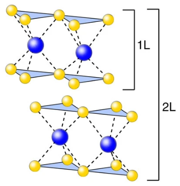
Lattice structures monolayer and bilayer. ©2014 Springer Nature Limited
Our research group has revealed the Photocarrier Relaxation Pathway in Two-Dimensional Semiconducting Transition Metal Dichalcogenides. We focus on how these atomically thin 2D crystals absorb a large fraction of incident photons in the visible frequencies, attributed to the ‘band nesting’ effect. Our work reveals that band nesting in mono- and bilayer MX2 (M = Mo, W; X = S, Se) results in excitation-dependent characteristic relaxation pathways of the photoexcited carriers. We found that photoexcited electron–hole pairs in the nesting region spontaneously separate in k-space, implying a temporary suppression of photocarrier loss due to direct exciton recombination. These findings highlight the potential for efficient hot carrier collection in optoelectronic devices.
Photocarrier relaxation pathway in two-dimensional semiconducting transition metal dichalcogenides.
Daichi Kozawa, Rajeev Kumar, Alexandra Carvalho, Kiran Kumar Amara, Weijie Zhao, Shunfeng Wang, Minglin Toh, Ricardo M. Ribeiro, A. H. Castro Neto, Kazunari Matsuda, Goki Eda.
Nature Communications, 5, 4543 (2014). 10.1038/ncomms5543