|
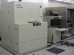
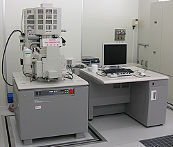
Double beam FIB–SEM hybrid system |
| |
|
Product |
Xvision200 |
Manufacturer |
SII Nanotechnology Corporation |
Capabilities |
FIB-gun Colum
Liquid Ga metal ion source
Acceleration voltage: 1 ~ 30kV (5kV step)
Maximum current density: 30A/cm2
Maximum scanning area: 2.0mm square
Image resolution: 4nm (acceleration voltage: 30kV)
EB-gun Colum
ZrO/W field emission type emitter
Acceleration voltage: 1 ~ 30kV
Maximum scanning area: 2.0mm square
Image resolution: 3nm (acceleration voltage: 5kV)
Sample Stage: X: 0 ~ 205mm Y: 0 ~ 205mm Z: 0 ~ 10mm θ: 360deg. T: -5 ~ +60deg.
Substrate sizes: 6" wafer, less than 3" wafer
Gas system for deposition ( Carbon )
Micro-probing system
|
|
| |
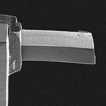
【Applications】 |
|
Fabrication of TEM sample |
|
|
|
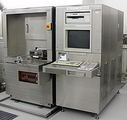
FIB system |
| |
|
Product |
SMI9800SE |
Manufacturer |
SII Nanotechnology Corporation |
Capabilities |
FIB-gun Colum
Liquid Ga metal ion source
Acceleration voltage: 15 ~ 30kV
Maximum current density: 10A/cm2
Maximum scanning area: 2.4mm square
Image resolution: 12nm (acceleration voltage: 30kV)
EB-gun Colum
ZrO/W field emission type emitter
Acceleration voltage: 0.5 ~ 25kV
Maximum scanning area: 1.0mm square
Image resolution: 3nm (acceleration voltage: 25kV), 10nm (acceleration voltage: 1kV)
Sample Stage: X: 0 ~ 200mm Y: 0 ~ 200mm Z: 0 ~ 14mm θ: 360deg. T: 0 ~ 90deg.
Substrate sizes: less than 8“ wafer
|
|
|
Field emission–scanning electron microscope(FE–SEM) |
| |
|
Product |
S-4800 |
Manufacturer |
Hitachi High-Technologies Corporation |
Capabilities |
EB gun: ZrO/W field emission type
Irradiation voltage: 0.5 ~ 30kV (normal mode), 0.1 ~ 2.0kV (retarding mode)
Resolution: 1.0nm @ 15kV (normal mode), 1.4nm @ 1.0kV (retarding mode), 2.0nm @ 1.0kV (normal mode)
Magnifications: 20 ~ 800,000
Sample stage moving area: X: 0 ~ 110mm Y: 0 ~ 110mm Z: 1.5 ~ 40mm R: 360deg. T: -5 ~ +70deg.
Maximum wafer size: 6“ wafer |
|
|
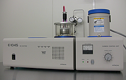
Coating system |
| |
|
Product |
E-1045 |
Manufacturer |
Hitachi High-Technologies Corporation |
Capabilities |
Metallurgical coating unit
Maximum voltage: DC 0.4kV
Maximum current: DC 40mA
Target material: Pt
Pressure: 7~20Pa
Timer: 5~300sec
Maximum sample size: diameter 60mm, height 20mm
Carbon coating unit
Voltage: AC 20V, 20A max
Target: Carbon
Distance between Target and Substrate: 50~80mm
Maximum sample size: diameter 60mm, height 20mm
|
|
|
Atomic force microscope(AFM) |
| |
|
Product |
L-traceⅡ |
Manufacturer |
SII Nanotechnology Corporation |
Capabilities |
Resolution: vertical 0.01 nm, surface 0.5 nm
Maximum wafer size: 6" ( thickness: 22 mm )
Scanning area: 90um
Sample moving area: X: ±75mm, Y: +105, -5mm, Z: 22mm
Scanning mode: AFM, FFM, DFM, PM, SIS
|
|
| |
【Applications】 |
|
|
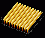
Observation of single carbon nanotube |
Observation of line pattern |
|
|
|
Auto ellipsometer |
| |
|
Product |
MARY-102FM |
Manufacturer |
- |
Capabilities |
Method : Rotating retarder method
Light source: 0.8mW He-Ne laser ( wavelength 632.8nm)
Beam diameter: 0.8mmφ
Incident angle: 50, 60, 70deg.
Accuracy: Δ=±0.01deg., Ψ=0.01deg.
Resolution: thickness 0.1Å
Sample stage: auto X, Y, θ
Moving area: ±50mm
XY drive resolution : 0.01mm
Maximum wafer size: 6“ wafer |
|
|
Surface profiler |
| |
|
Product |
Alpha-Step IQ |
Manufacturer |
KLA-Tencor Corporation |
Capabilities |
Resolution: 1.19pm (±10um range) / 23.8pm (400um range)
Maximum wafer size: 6“ wafer
Scan length: 10mm
Measurement range of thickness: ~400um
Repeatability: 8Å@1 sigma (guaranteed)
Moving area: X 150mm, Y 80mm, θ 360deg.
Sampling rate: 2,5, 10, 20, 50, 100, 200um/s |
|
|
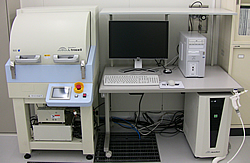
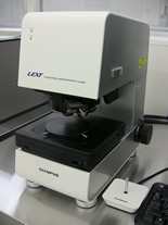
3D-measurement laser microscope (operated by LCnet Project) |
| |
|
Product |
LEXT OLS4000 |
Manufacturer |
Olympus Corporation |
Capabilities |
It is possible to...
1. get high resolution images by a 405nm semiconductor laser
2. observe bright-field images by a white light source
3. perform a differential interference observation by both laser and white light source
4. use for any samples of varied sizes, materials, and shape.
5. perform non-contact 2D and 3D measurements.
6. obtain accurate measured values. (2D: < ±2%, 3D: < 0.2+L /100um) |
|
|