 |
 |

|
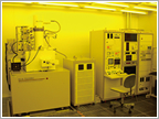
Facility
・Clean room with total area around 450m2
・Non-clean room laboratory around 40m2 for device characterization, cutting, and polishing process
Handling Materials
Compound semiconductors, Silicon, Oxide, Magnetic, Metal materials
Function
Three-dimensional processing such as Photonic crystal, Nano carbons, etc.
Main System
Electron beam & laser lithography, ICP-RIE, Bosch, W-beam FIB, etc. |
| |
 |
 |
 |
 |
 |

 |
|
 |
|
|
|
 |
 |
 Japan’s "Nanotechnology Network" is a Program sponsored by the Ministry of Education, Culture, Sports, Science and Technology (MEXT). For five years starting from year 2007, academic, business, and governmental nanotechnology researchers will have the opportunity to use facilities and equipment at 13 network sites with cutting edge nanotechnology. The aim of this Program is to generate research results that will lead to innovations. Fourteen institutions participated in "Nanotechnology Support Project" in the previous term. Now, the number has been greatly increased, and 13 sites and 26 institutions are participating in "Nanotechnology Network", enabling high-level technical support in nanotechnology to various requests from the research community. "NIMS Center for Nanotechnology Network" will provide support in the three out of four areas designated by MEXT to cover in the Program - "Nano-characterization", "Nano-fabrication", and "Extreme Conditions". Continuing from the previous term, we have agreed to function as a center, or a representative and a coordinator of the nation-wide network.
|
|


