National Institute for Materials Science
文字サイズ small   middle   large   Japanese
NIF
Flow of Use Contact User Login Downloads Access Links
HOME > 3-D Nano-Integration Foundry > Examples in our facility
  Examples in our facility
 
Accomplishment
Development of full color filter using surface plasmons
SEM image(left) and transmitted light image (right) of the fabricated full color filter.
 
SEM image of the measured device with electrode assignment. Bright areas show etched triple-layer graphene. The two isolated islands (quantum dots) are connected via two narrow constrictions to wide source and drain regions.
 
Charge stability diagrams for series-coupled quantum dots. Color scale plot of the transconductance (dI/dVg1) calculated from dc current (I) as a function of Vg1 and Vg2 at Vsd = 50 μV.
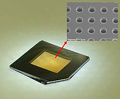
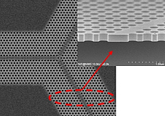
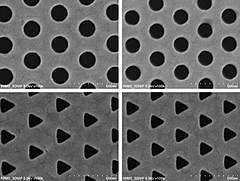
It was possible to form a nanoscale hole array with extremely accurate periodicity using the electron-beam lithography method and reactive ion etching method by adopting aluminum as a metal material with which surface plasmon resonance can be obtained in the entire visible light region, resulting in the successful development of a color filter for the five colors red, orange, yellow, green, and blue. The newly-developed device displays excellent monochromaticity and transmittance.
Realization of coupled quantum dot device using three layers of graphene
 
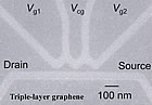
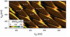
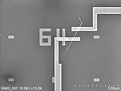
Two quantum dots in close proximity, which confine electrons, and the device structure that controls electrical transmission, including electrodes, etc., were all fabricated in a single graphene sheet by direct processing of a graphene sheet consisting of three layers of graphene (thickness: approximately 1nm) using the electron beam lithography and reactive ion etching techniques. The researchers also succeeded in demonstrating single electron device operation, in which the electrons in the quantum dots are transferred individually, and in modifying the coupling of the electrons between the two quantum dots utilizing the graphene gate electrode. As a result, this work realized a coupled quantum dot device,
which is the most fundamental integrated nanodevice.
“Nano Letters” in press

Practical example
SiO2 cantilever structure
 
Contact electrodes on graphene
 
Contact electrodes on single nanowire
SiO2 cantilever structure
 
Contact electrodes on graphene
 
Contact electrodes on single nanowire

LaB6 emitter using FIB
 
TEM sample using FIB
 
Si stencil mask

Si stencil mask
LaB6 emitter using FIB
(NIMS,1D Nanomaterials Group, Jie Tang)
 
TEM sample using FIB
   

GaAs photonic crystal waveguide
 
Si deep etching using Bosch process
 
GaAs MESFET
GaAs photonic crystal waveguide
 
Si deep etching using Bosch process
 
GaAs MESFET

Sub-wavelength diameter air-holes of Al thin film
 
Through holes in Si wafer
 
Random-size pillar structure of SiO2
Sub-wavelength diameter air-holes of Al thin film
 
Through holes in Si wafer
(thickness: 380um)
 
Random-size pillar structure of SiO2

Diamond emitter
 
Diamond etching
 
Three-dimensional visualization of cementite lamellae
Diamond emitter
 
Diamond etching
 
Three-dimensional visualization of cementite lamellae

HOME