| |
■
メンバー
| 三木一司 ディレクター
MIKI Kazuhsi, Director |
 |
| |
 |
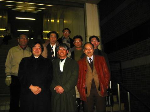 |
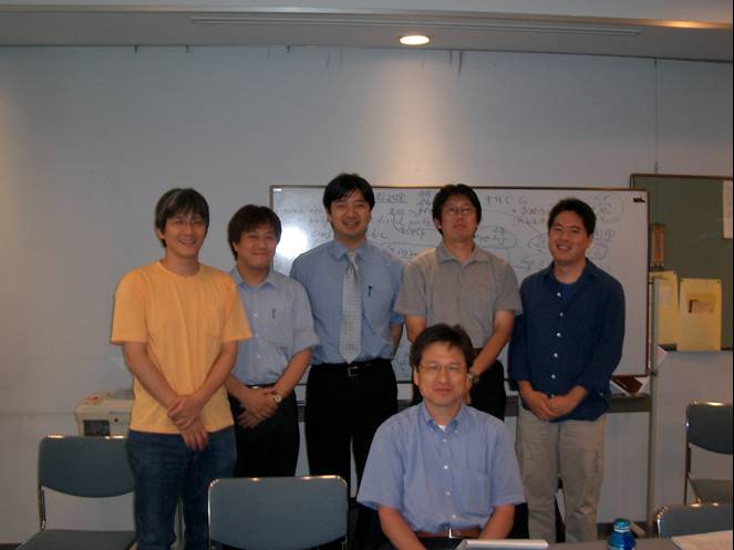
| 某ミーティングにて
|
2004年冬長岡技術科学大学での招待講演の後 |
物質・材料研究機構ナノ有機センター
グループリーダ&ディレクター(ナノアーキテクチャーグループ)
〒305−0044 茨城県つくば市並木1−1
(ナノ・生体材料研究棟226室)
miki.kazushi@nims.go.jp
(秘書宛 Tanaka.masayo@nims.go.jp )
電話・ファックス 029-860-4718
筑波大学 数理物質科学研究科 物質・材料工学専攻 准教授(連携) 兼任
産業技術総合研究所 エレクトロニクス研究部門、ナノテクノロジー研究部門 客員研究員 併任
チェコ共和国 カレル大学 客員教授
Director, Nano-Architecture Group,
Organic Nanomaterials Cente,
National Institute for Materials Science (NIMS)
1-1 Namiki, Tsukuba.
Ibaraki 305-0044, Japan
e-mail: miki.kazushi@nims.go.jp
(our secretary, Ms. Tanaka: tanaka.masayo@nims.go.jp)
Phone & telfax +81-29-860-4718
Associate Professor, University of Tsukuba
Doctroral Program in
Materials Science and Engineering
Garduate School of Pure and
Applied Sciences
Senior Researcher,
Nanoelectronics Institute & Nanotechnology Institute, National
Institute of Advanced Industrial Science and Technology (AIST)
 経歴 経歴
最終学歴 1987 年 3 月 筑波大学工学研究科博士課程修了 工学博士(筑波大学)
学位論文名「電子分光法による炭素同素体の電子構造の研究」(指導教官 小間篤、主査 壽榮松宏)
学歴
1978 年 3 月 兵庫県立姫路東高等学校卒業
1978 年 4 月 筑波大学第3学群基礎工学類(主専攻変換工学)入学
1982 年 3 月 同大学同学群同学類卒業
1982 年 4 月 筑波大学大学院博士課程工学研究科(物質工学専攻)入学
1984 年 3 月 同研究科(物質工学専攻)にて工学修士取得
1987 年 3 月 同研究科(物質工学専攻)修了、工学博士取得
職歴・研究活動の経歴
1987 年 4 月 通商産業省工業技術院 電子技術総合研究所入所(電子デバイス部)
(国家公務員試験 I 種電子工学合格として採用)
1987 年〜 1990 年 超格子素子の研究開発(通商産業省次世代産業基盤技術研究開発制度) 従事
1987 年〜 1990 年 マイクロエレクトロニクス STM 技術の研究(通商産業省官民連帯共同研究制度)従事
1991 年 10 月 通商産業省工業技術院 電子技術総合研究所 主任研究官
1991 年〜 2000 年 超高効率太陽電池の研究開発(通商産業省ニューサンシャイン計画) 従事
1994 年 9 月〜 1995 年 8 月 科学技術庁長期在外研究員(オックスフォード大学) として派遣
‘ 半導体表面の走査型トンネル顕微鏡観察の研究
'
1995 年 10 月〜 1996 年 5 月 オックスフォード大学客員研究員
1997 年 4 月〜 1998 年 3 月 通商産業省工業技術院 研究開発官(電子・情報・通信担当)付
1999 年 脱気技術を用いた半導体デバイス作製用超純水装置実用化に関する研究開発
研究リーダ(通商産業省工業技術院重要技術の競争的研究開発)
1999 年 通商産業省工業技術院 電子技術総合研究所 ラボリーダ
1999 年〜 2000 年 高信頼性シリコン酸化膜実現に関する研究 研究リーダ
(通商産業省工業技術院重要技術の競争的研究開発)
2000 年〜 新しい情報プラットフォームのためのアクティブ原子配線網に関する研究 サブリーダ
(文部科学省 科学技術振興調整費 総合研究)
2001 年 1 月 4 日 行政改革により経済産業省産業技術総合研究所 電子技術総合研究所(主任研究官)に配置換え
2001 年 4 月 1 日 行政改革により経済産業省 独立行政法人産業技術総合研究所(ナノテクノロジー研究部門 主任研究員)に配置換え
2001 年 7 月 1 日 独立行政法人物質・材料研究機構 客員研究員
〜 2002 年 3 月 31 日
2001 年 4 月 1 日 独立行政法人物質・材料研究機構 ナノマテリアル研究所主席研究員
2003 年 1 月 24 日 独立行政法人物質・材料研究機構 ナノマテリアル研究所ディレクター
2005 年 4 月 1 日 独立行政法人物質・材料研究機構 ナノ有機センターグループリーダ
〜現在 (ナノアーキテクチャーグループ)
産業技術総合研究所併任(エレクトロニクス研究部門、ナノテクノロジー研究部門 客員研究員)
所属学会
米国物理学会、米国真空学会、日本応用物理学会
主な学会活動
日本応用物理学会 応用物性(熱電変換)世話人 2000.4.1--2004.3
日本応用物理学会 応用物性 代表世話人 2002.4.1-2004.3
日本応用物理学会 講演会企画委員会委員;若手奨励賞審査委員会委員 2002.4.1-2004.3
日本応用物理学会 シリコンテクノロジー分科会 常任幹事 2001.4-2002.3
日本応用物理学会 シリコンテクノロジー分科会 幹事( Si ナノテクノロジー研究委員会) 2002.4-2004.3
日本応用物理学会 薄膜表面分科会 幹事 2003.4-2005.3
日本表面科学会 学会誌「表面科学」編集委員 2000.4.1-2002.3
新技術振興事業団「高機能薄膜デバイス研究会」((財)新技術振興渡辺記念会の委託)委員 2001.12.1-2002.3.31; 「ナノデバイス研究会」
2002.4.1-2003.3.31
Japanese Journal of Applied Physics 特集号(アジア太平洋表面界面分析会議 APSIAC ' 02
)特別編集委員、
2002.10-
主な国際学会活動
Asia-Pacific Surface & Interface Analysis Conference (APSIAC02)
論文委員、会期 10 月 2 日− 4 日,東京大学(本郷)
MRS-Africa International Committee
2002-
受賞歴、表彰歴
1994 年 10 月〜 1996 年 5 月 オックスフォード大学 Visiting Scholar (Wolfson College)
2000 年 7 月 電子技術総合研究所 業務表彰 業績賞「先端シリコンプロセス技術の開発と原子配線網応用に関する研究」
研究経験
結晶成長( MBE )、電子分光( AES ,エネルギー損失分光)、電子線回折( RHEED 、 LEED )、走査型プローブ顕微鏡(
STM , AFM )、電子顕微鏡( SEM )、ダイシング ソー、光学リソグラフィー、熱酸化炉・アニール炉、RIE、超純水装置、蒸着装置、プログラム言語(
C 、 BASIC )等
研究成果等
研究論文数 82 編(英文 80 編、和文2編)
プロシーディングス数 82 編(英文 80 編、和文2編)
口頭発表数 82 編(英文 80 編、和文 205 編)
その他発表数 82 編(英文 80 編、和文2編)
資格
一般高圧ガス主任管理者(乙種機械) 1990 年 2 月 14 日取得
特殊高圧ガス主任管理者 1996 年 11 月 1 日取得
健康状態
良好
趣味
バドミントン(ダブルス)、スキー(初級者)、登山、酒全て(ワインティスティング等)、料理(肉、魚、パスタ、中華、デザート)、スキューバダイビング(オープンウォ
ター)、フィギュア−スケート、ガーデニング、旅行(ヨーロッパ、アフリカ、中国、オーストラリア、ニュージランド)、油絵
家族
妻、娘一人
主な共同研究者
Andrew Briggs オックスフォード大学材料科学部 教授
山部紀久夫 筑波大学物理工学系 教授
山崎 聡 産業技術総合研究所 新炭素系材料研究開発センター 総括研究員
Publication list
surface science, crystal growth, nanoscience/technology
○ publications major journals (-2010)
○ conference proceedings (-2004)
Nov.30, 2010
Publication in major journal
' Core Excitation
Spectra of Diamond, Graphite and Glassy Carbon. Applied Physics
A34 (1984) 35-39. A. Koma and K. Miki. Core Excitation
Spectra of Diamond, Graphite and Glassy Carbon. Applied Physics
A34 (1984) 35-39. A. Koma and K. Miki.
Low-Energy Electron
Energy Loss Spectroscopy on C8K. 'Graphite Intercalation Compounds
- Recent Progress of Research in Japan' , edited by S. Tanuma
and H. Kamimura (World Scientific, Singapore, 1985). pp. 226-235.
A. Koma, K. Miki, and H. Suematsu,
High Density
Molecule-Like Species Formed in Surface Layer of C8K. Synthetic
Metals 12 (1985) 269-274. K. Miki, H. Suematsu, and A. Koma.
Density-of-States
Investigation of C8K and Occurrence of the Interlayer Band. Physical
Review B34 (1986) 2434-2438. A. Koma, K. Miki, H. Suematsu
T. Ohno, and H. Kamimura.
Imaging of
Hydrogen-Induced Si(111)-Surface with the Scanning Tunneling Microscopy.
J. Microscopy 133 (1988) H. Tokumoto, K. Miki, H. Murakami,
Y. Morita, H. Bando, A. Sakai, S. Wakiyama, M. Ono, and K. Kajimura.
Photoluminescence
Study on Initial Stage of GaAs Growth on Si. Journal of Vacuum
Science & Technology B7 (1989) 481-486. H. Okumura, Y.
Suzuki, K. Miki, K. Sakamoto, T. Sakamoto, S. Misawa and S. Yoshida.
Gem/Sin Strained-Layer
Superlattices Fabricated by Phase-Locked Epitaxy. Journal of
Crystal Growth 95 (1989) 444-446. K. Miki, K. Sakamoto, T.
Sakamoto, H. Okumura, N. Takahashi, and S. Yoshida.
Raman Scattering and Photoluminescence Characterization of Ge/Si
Strained-Layer Superlattices Grown by Phase-Locked Epitaxy. Applied
Surface Science 41/42 (1989) 548-552. H. Okumura, K. Miki,
K. Sakamoto, T. Sakamoto, K. Endo, and S. Yoshida.
Surface Step Structure
of a Lens-Shaped Si(001) Vicinal Substrate. Thin Solid Films
183 (1989) 229-233. K. Sakamoto, K. Miki and T. Sakamoto,
Observation
of Si(001) Vicinal Surfaces on RHEED. Journal of the Electrochemical
Society 136 (1989) 2705-2710. K. Sakamoto, K. Miki, T. Sakamoto,
and S. Nagao.
Scanning Tunneling
Microscopy on a Si(001)-2x1 Surface. Japanese Journal of Applied
Physics 28 (1989) L1487-L1485; Errata 28 (1989)
L2107. K. Miki, H. Tokumoto, T. Sakamoto and K. Kajimura.
Observation
of direct band gap properties in GenSim strained-layer superlattices.
Japanese Journal of Applied Physics 28 (1989) L1893-L1895.
H. Okumura, K. Miki, S. Misawa, K. Sakamoto, T. Sakamoto, and S.
Yoshida.
Electro- and photoreflectance
of ultrathin Ge/Si superlattices grown by phase-locked epitaxy.
Japanese Journal of Applied Physics Part 2 29 (1990) L381-L384.
K. Asami, K. Miki, K. Sakamoto, T. Sakamoto, and S. Gonda.
Real-time Observation
of Oxygen and Hydrogen Adsorption on Silicon Surfaces by Scanning
Tunneling Microscopy. Journal of Vacuum Science & Technology
A8 (1990) 255-258. H. Tokumoto, K. Miki, H. Murakami, H. Bando,
M. Ono, and K. Kajimura,
Scanning Tunneling
Microscopy of [11-2] Oriented Steps on a Cleaved Si(111) Surface.
Applied Physics Letters 56 (1990) 743-745. H. Tokumoto,
S. Wakiyama, K. Miki, and S. Okayama.
Anisotropic
Surface Migration during MBE on Stepped Surfaces of Vicinal Si(111).
Journal of Crystal Growth 99 (1990) 510-513. K. Sakamoto,
K. Miki and T. Sakamoto
STM Images of Anisotropy
Atomic Steps on Si(111)-7x7 Surfaces. Journal of Crystal Growth
99 (1990) 1329-1332. H. Tokumoto, K. Miki, and K. Kajimura
Structure Dependence
of Photoluminescence in GenSim Strained-Layer Superlattices. Journal
of Crystal Growth 111 (1991) 902-906. K. Miki, H. Okumura,
K. Sakamoto, H. Matsuhata T. Sakamoto, and S. Yoshida.
Step stability,
domain coverage, and nonequilibrium kinetics in Si (001) molecular-beam
epitaxy. Physical Review B, Condens. Matter 41 (1990)
10198-10201. S. Clarke, M.R. Wilby, D.D. Vvedensky, T. Kawamura,
K. Miki, H. Tokumoto.
Direct Observation
of SiH 3 on a 1%-HF-treated Si(111) Surface by Scanning Tunneling
Microscopy. Applied Physics Letter 59 (1991) 1347-1349.
Y. Morita, K. Miki and H. Tokumoto
Scanning Tunneling
Microscopy of Microstructure on Cleaved Si(111) Surface. Journal
of Vacuum Science & Technology B9 (1991) 695-698. H. Tokumoto,
S. Wakiyama, K. Miki, H. Murakami, S. Okayama, and K. Kajimura
Heating Current-Induced
Step Motion on Si(111) Surface by Scanning Tunneling Microscopy.
Journal of Vacuum Science & Technology B9 (1991) 699-702.
H. Tokumoto, K. Miki, H. Murakami, and K. Kajimura
Photoluminescence
and Electroreflectance of Ge-Si Strained Layer Superlattices. Materials
Science and Engineering B9 (1991) 245-248. H. Okumura, K.
Miki, S. Misawa, K. Sakamoto, T. Sakamoto, S. Yoshida, K. Asami
and S. Gonda
Observation
of Micro-Structure in Si12/Ge4 and Si18/Ge6 Strained layer superlattice.
Electron microscopy and Microanalysis Group 91 (1991).
H. Matsuhata, K. Miki, S. Unoki, K. Sakamoto, and T. Sakamoto.
Atomic Structures
of Hydrogen-Terminated Si(111) Surfaces by Hydrofluoric Acid Treatments.
Japanese Journal of Applied Physics Part 1 30 (1991) 3570-3574.
Y. Morita, K. Miki and H. Tokumoto.
Atomic Scale Analyses
of HF-Treated Si(111) Surfaces by STM. Applied Surface Science
60/61 (1992) 466-473. Y. Morita, K. Miki and H. Tokumoto,
Thermal Stability
of Si/Gen/Si Heterostructures by Photoreflectance. Journal of
Electronics Materials 21 (1992) 223-226. K. Asami, K. Miki,
K. Sakamoto, T. Sakamoto, and S. Gonda,
Step Control
on Silicon Surfaces by Electric Fields. Nanotechnology
3 (1992) 142-144. K. Miki and H. Tokumoto,
Real Time Observation
of Si(111):(7x7)-(1x1) Phase Transition by Scanning Tunneling Microscopy.
Ultramicroscopy 42-44 (1992) 851-857. K. Miki, Y. Morita,
H. Tokumoto, T. Sato, M. Iwatsuki, M. Suzuki, and T. Fukuda.
Real Time Observation
of Step Motion on Si(111) Surface by Scanning Tunneling Microscopy.
Ultramicroscopy 42-44 (1992) 816-823. H. Tokumoto, K.
Miki, Y. Morita, T. Sato, M. Iwatsuki, M. Suzuki, and T. Fukuda.
Scanning Tunneling
Microscopy of 1%-HF-Treated Si(111) Surfaces. Ultramicroscopy
42-44 (1992) 822-827. Y. Morita, K. Miki and H. Tokumoto.
Ge Distribution
in Gen/Si m Strained-Layer Superlattices. Japanese Journal
of Applied Physics 31 (1992) L1511-L1513. K. Miki, S. Unoki,
H. Matsuhata, K. Sakamoto, and T. Sakamoto.
Effect of a
surfactant on the growth of Si/Ge heterostructures. Thin Solid
Films 222 (1992) 112-115. K. Sakamoto, K. Miki, T. Sakamoto,
H. Yamaguchi, H. Oyanagi, H. Matsuhata, and K. Kyoya.
Which Surfactant
Shall We Choose for the Heteroepitaxy of Ge/Si(001)? - Bi as a Surfactant
with Small Self-Incorporation -. Journal of Applied Physics
32 (1993) L204-L206. K. Sakamoto, K. Kyoya, K. Miki, H. Matsuhata,
and T. Sakamoto.
Microstructure
in molecular-beam-epitaxy-grown Si/Ge short-period strained-layer
superlattices. Physical Review B47 (1993) 10474-10483.
H. Matsuhata, K. Miki, K. Sakamoto, T. Sakamoto, and S. Yoshida.
High temperature
scanning tunneling microscopy observation of phase transition and
reconstruction on a vicinal Si(111) surface. Physical Review
B47 (1993) 13027-13033. H. Hibino, T. Fukuda, M.Suzuki, Y.
Homma, T. Sato, M. Iwatsuki, K. Miki, and H. Tokumoto.
Effect of surfactants
on surface migration in Si MBE. Journal of Crystal Growth
127 (1993) 392-395. K. Sakamoto, K. Miki, T. Sakamoto, H. Matsuhata,
and K. Kyoya.
Si(111)- √ 3x √ 3 R30: Si Mediated by Hydrogen.
Surf. Sci . 298, L163-L168 (1993). Y. Morita, K. Miki,
H. Tokumoto.
Real Time Observation
of (1x1)-(7x7) Phase Transition on Vicinal Si(111) Surfaces by Scanning
Tunneling Microscopy. Japanese Journal of Applied Physics
32 (1993) 3247-3251. M. Suzuki, H. Hibino, Y. Homma, T. Fukuda,
T. Sato, M. Iwatsuki, K. Miki, and H. Tokumoto.
Real-time Scanning
Tunneling Microscopy of Phase Transition and Faceting on a Vicinal
Si(111). J. Vac. Sci. & Technol. A11 (1993) 1640-1643.
M. Suzuki, T. Homma, H. Hibino, T. Fukuda, T. Sato, M. Iwatsuki,
K. Miki, and H. Tokumoto.
Abrupt Si/Ge/Si(001)
Interfaces Fabricated with Bi as a Surfactant. Japanese Journal
of Applied Physics B33 (1994) 2307-2310. K. Sakamoto, H. Matsuhata,
K. Kyoya, K. Miki, and T. Sakamoto.
Nucleation and Coalescence
in Hydrogenated Amorphous Silicon Studied by Scanning Tunneling
Microscopy. Appl. Phys. Lett. 65 (1994) 1760-1762. K.
Ikuta, K. Tanaka, S. Yamasaki, K. Miki and A. Matsuda.
Kinetics of hydrogen
desorption on a Si(111) surface. Surf. Sci. 325 (1995)
21-32. Y. Morita, K. Miki and H. Tokumoto.
Electrochemical
scanning tunneling microscopy and atomic force microscopy observations
on Si(111) in several solutions. Japanese Journal of Applied
Physics B34 (1995) 715-718. A. Ando, K. Miki, T. Shimizu, K.
Matsumoto, Y. Morita and H. Tokumoto.
Adsorption and desorption
of atomic hydrogen on Si(001) and its effects on Si MBE J. Cryst.
Growth 157, 295-9 (1995). K. Sakamoto, H. Matsuhata, K. Miki,
T. Sakamoto.
Identification
of the Si(001) missing dimer defect structure by low bias voltage
STM and LDA modelling. Surf. Sci. 341 (1995) L1042-1047.
J.H.G. Owen, D.R. Bowler, C.M. Goringe, K. Miki
and G.A.D. Briggs.
Surface observation
and modification of Si substrate in NH4F and H2O solutions. Jpn.
J. Appl. Phys. 35 (1996) 1064-8. A. Ando, K. Miki, K. Matsumoto,
T. Shimizu, Y. Morita and H. Tokumoto.
Hydrogen diffusion
on Si(001). Phys. Rev. B54 (1996) 14153-14157. J.H.G. Owen,
D.R. Bowler, C.M. Goringe, K. Miki and G.A.D. Briggs.
Spatially controlled
formation of an atomically flat Si(001) surface by annealing with
a direct current in an ultrahigh vacuum. Jpn. J. Appl. Phys.
36 (1997) 1424-1427. A. Ando, K. Sakamoto, K. Miki, K. Matsumoto
and T. Sakamoto.
Is the c(4x4)
reconstruction of Si(001) associated with the presence of carbon?
Appl. Phys. Lett. 71 (1997) 3266-8. K. Miki, K. Sakamoto,
T. Sakamoto.
A proposed
structure of the nucleus for gas-source epitaxial growth of Group
IV semiconductors. Surf. Sci. 382 (1997) L678-685. J.H.G. Owen,
D.R. Bowler, C.M. Goringe, K. Miki and G.A.D. Briggs.
Gas-source growth
of Group IV semiconductors: 1. Si(001) nucleation mechanisms. Surf.
Sci. 394 (1997) 79-90. J.H.G. Owen, K. Miki, D.R. Bowler,
C.M. Goringe, I. Goldfarb and G.A.D. Briggs.
Gas-source growth
of Group IV semiconductors: 2. Growth regimes and the effect of
hydrogen. Surf. Sci. 394, 91-104 (1997). J.H.G. Owen,
K. Miki, D.R. Bowler, C.M. Goringe, I. Goldfarb and
G.A.D. Briggs.
Gas-source growth
of Group IV semiconductors: 3. Nucleation and growth of Ge/Si(001).
Surf. Sci. 394 (1997) 105-118. I. Goldfarb, J.H.G. Owen,
P.T. Hayden, K. Miki and G.A.D. Briggs.
In situ observation
of gas-source molecular beam epitaxy of silicon and germanium on
Si(001). J. Vac. Sci. Technol. A, Vac. Surf. Films 16
(1998) 1938-1943. I. Goldfarb, J.H.G. Owen, D.R. Bowler, C.M. Goringe,
P.T. Hayden, K. Miki, D.G. Pettifor, G.A.D. Briggs.
Surface Preparation
of Si Substrates for Epitaxial Growth. Surf. Sci 406 (1998)
312-327. K. Miki, K. Sakamoto, and T. Sakamoto.
Formation and
characterization of thin oxide layers on the spatially controlled
atomic-step-free Si(001) surface. Jpn. J. Appl. Phys. Part 1
37 (1998) 1680-1683. A. Ando, K. Sakamoto, K. Miki, K. Matsumoto,
T. Sakamoto.
Oxidation of spatially
controlled atomically flat Si(001) surface. Appl. Surf. Sci.
130-132 (1998) 197-201. A. Ando, K. Sakamoto, K. Miki, K.
Matsumoto, T. Sakamoto.
Diffusion of paired
hydrogen on Si(001). Phys. Rev. B57 (1998) 8790. D.R. Bowler,
J.H.G. Owen, K. Miki, and G.A.D. Briggs.
Bi Induced Structures
on Si(001) Surfaces. Surf. Sci. 421 (1999) 397-418. K.
Miki, J.H.G. Owen, D.R. Bowler, G.A.D. Briggs, and K.
Sakamoto.
Characterization
of ultrathin SiO x layers formed on a spatially controlled atomic-step-free
Si(001) surface. Appl. Surf. Sci. 144-145 (1999) 589-592.
A. Ando, K. Sakamoto, K. Miki, K. Matsumoto, T. Sakamoto.
Atomically
Perfect Bismuth Line on Si(001) by Selective Desorption Process.
Phys. Rev. B59 (1999) 14868. K. Miki, D.R.
Bowler, J.H.G. Owen, G.A.D. Briggs, and K. Sakamoto.
Interface States
of SiO2/Si(111) Observed by an Atomic Force Microscope. Surface
Science 443 (1999) L1055-L1058 . R. Hasunuma, Y.
Nishioka, A. Ando and K. Miki.
Bismuth and
Antimony Nanolines in Si Epitaxial Layer. Microscopy of Semiconducitng
Materials 1999 (Edited by A G Cullis, and J L Hutchison), Inst.
Phys. Conf. Ser. 164 (1999) 167-170. K. Miki,
H. Matsuhata, K. Sakamoto, J.H.G. Owen, D.R. Bowler, and G.A.D. Briggs.
Structures
of the “nano-wire” and 2xn of Bi/Si(001). Surf. Sci. Lett. (1999).
Surface Science 447 (2000) L169-L174 . M. Shimomura,
K. Miki, T. Abukawa and S. Kono.
Conducting atomic
force microscopy studies on local electrical properties of ultrathin
SiO2 films. Appl. Surf. Sci. 162-163 (2000) 401-405. A.
Ando, R. Hasunuma, T. Maeda, K. Sakamoto, K. Miki, Y. Nishioka and
T. Sakamoto.
Analysis on Interface
States of Ultrathin-SiO2/Si(111) Interface. Appl. Surf. Sci
. 159-160 (2000) 83-88. R. Hasunuma, A. Ando, K. Miki and Y.
Nishioka.
Analysis on Electronic
Properties of Ultrathin- SiO2/Si(111) Interface with an Atomic Force
Microscope. Appl. Surf. Sci . 162-163 (2000) 547-552. R.
Hasunuma, A. Ando, K. Miki and Y. Nishioka.
An Experimental-Theoretical
Study of the Behavior of Hydrogen on the Si(001) Surface. J.
Phys.: Condens. Matter. 12 (2000) 7655-7670. D.R. Bowler,
J.H.G. Owen, C.M. Goringe, K. Miki and G.A.D. Briggs.
Conducting-AFM
spectroscopy on Ultrathin SiO2 Films. Appl. Phys . A Materials
Science and Processing 72 (2001) S223-S226. A. Ando, K. Miki,
R. Hasunuma, and Y. Nishioka.
Bi nanoline
passivity to attack by atomic oxygen or hydrogen. Surf. Sci.
499 (2002) L124-L128. J.H.G. Owen, D.R. Bowler, and K. Miki.
Origin of type-C_
defects on the Si(100)-(2x1) surface. Phys. Rev. B65
(2002) 161302( R ). M. Nishizawa, T. Yasuda, S. Yamasaki, K.
Miki, M. Shinohara, N. Kamakura, Y. Kimura and M. Niwano.
Stress relief
as the driving force for self-assembled Bi nanolines. Phys.
Rev. Lett . 88 (2002) 226104. J.H.G. Owen, K. Miki, H. Koh,
H.W. Yoem and D.R. Bowler.
74.
Leakage Current
Distribution of Cu-Contaminated Thin SiO2. Jpn. J. Appl. Phys.
Part 2. 42 (2003) No.2B.pp.L160-L162 Norio Tokuda, Takahiro
Kanda, Satoshi Yamasaki, Kazushi Miki and Kikuo Yamabe.
Interaction between
electronic structure and strain in Bi nanolines on Si(001). Surf.
Sci . 527,no. 1-3 L177-L183 (2003). J.H.G. Owen, K. Miki, D.R.
Bowler.
A probe-positioning
method with two dimensional calibration pattern for micro-multi-point
probes Rev. Sci. Inst. 74, no.5 2722-2725 (2003). W. Yashiro,
I. Shiraki, and K. Miki
Si Submonolayer
and Monolayer Digital Growth Operation Techniques Using Si2H6 as
Atomically Controlled Growth Nanotechnology. Appl. Surf. Sci.
216(2003) 424-430. Y. Suda, N. Hosoya, K. Miki.
Selective Growth
of Cu Nanowires on Si(111) Substrates. Jpn. J. Appl. Phys. Part
2. 42 (2003) No.10A. pp.L1210-L1212. Norio Tokuda, Daisuke
Hojo, Satoshi Yamasaki, Kazushi Miki and Kikuo Yamabe.
Local Dielectric
Degradation of Cu-Contaminated SiO2 Thin Films. Solid State
Phenomena (2003) N,Tokuda, S.Yamasaki, K.Miki, K.Yamabe
Structural Analysis
of Bismuth Nanowire by X-Ray Standing Wave Method Jpn. J. Appl.
Phys. Part 1-Regular Papers Short Notes & Review Papers. 42
(2003) No.4B. pp.2408-2411. Akira Saito, Kenji Matoba, Tomoki Kurata,
Junpei Maruyama, Yuji Kuwahara, Kazushi Miki and Masakazu Aono .
New method
to characterize mesoscopic-range and very small strain with using
multi-wave x-ray diffraction. Surf. Sci. 550.1-3 (2004)
93-105. W. Yashiro, K. Sumitani, T. Takahashi, Y. Yoda, K. Miki.
STM-induced molecular
fluorescence from porphyrin molecules on metal substrates. Appl.
Phys. A - Materials Science & Processing Online First [DOI: 10.1007/s00339-004-2896-3].
Z-C. Dong, X.-L. Guo, A.S. Trifonov, P.S. Dorozhkin, K. Miki, K.
Kimura, S. Yokoyama and S. Mashiko
Electron-Stimulated
Athermal Surface Recrystallization of Si(100). J. Phys.: Condens.
Matter, 4. L193-L200 (2004). T. Narushima, M. Kitajima and
K. Miki.
Vibrationally Resolved
Fluorescence from Organic Molecules near Metal Surfaces Induced
by a Scanning Tunneling Microscope. Phys. Rev. Lett .92
(2004)086801-1-086801-4. Z-C. Dong, X.-L. Guo, A.S. Trifonov, P.S.
Dorozhkin, K. Miki, K. Kimura, S. Yokoyama and S. Mashiko
Fabrication
of Cu nanowires along atomic step edge lines on Si(111) substrates.
Appl. Surf. Sci. 237 (2004) pp. 528-531. Norio Tokuda,
Hidenobu Watanabe, Daisuke Hojo, Satoshi Yamasaki, Kazushi Miki
and Kikuo Yamabe.
Molecular fluorescence
from ZnTBP porphyrin molecular layers on Cu(100) induced by tunneling
currents. Nanotechnology 15-6 (2004) pp.402-405. X.-L.
Guo, Z-C. Dong, A.S. Trifonov, K. Miki, S. Mashiko, and T. Okamoto.
STM-induced light emission from the surface of H2TBP porphyrin/PEP porphyrin/Cu(100). Appl. Surf. Sci. 241 (2005) pp. 28-32; Erratum Appl. Surf. Sci. ?? (2005) pp. ??. X.-L. Guo, Z-C. Dong, A.S. Trifonov, K. Miki, K. Kimura, and S. Mashiko.
Determination method of crystal orientation by an area-detector image for surface X-ray direction. Journal of Applied Crystallography 38(2005) pp.319-323. W. Yashiro, S. Kusano, and K. Miki.
Encapsulation of atomic-scale Bi wires in epitaxial silicon without loss of structure. Physical Review B 72 (2005) pp. 121407(R )-1-121407(R )-4. Osami Sakata, Wataru Yashiro, D.R. Bowler, Kunihiro Sakamoto, and Kazushi Miki.
Electronic structure of a polymer nanowire on H-terminated Si(100). J. Appl. Phys 97(2005) pp.124302-1-124302-6. Yasuhiro Terada, Kazushi Miki, Masaaki Fujimori, Seiji Suwa, and Tomihiro Hashizume.
Selective Growth of Ag Nanowires on Si(111) Surfaces by Electroless Deposition. Journal of Physical Chemistry B 109 (2005) pp.12655-12657. N. Tokuda, N. Sasaki, H. Watanabe, K. Miki, S. Yamazaki, R. Hasunuma and K. Yamabe
NH3 on Si(001): Self-organized patterns of adsorbates investigated by a combination of scanning tunneling microscopy experiments and density functional theory calculations. Physical Review B 72 (2005) pp. 113304-1-113304-4. J. H. G. Owen, D. R. Bowler, S. Kusano and K. Miki
STM-induced molecular fluorescence from porphyrin molecules on metal substrates. Appl. Phys. A - Materials Science & Processing 81-2 (2005) pp367-370. Z-C. Dong, X.-L. Guo, A.S. Trifonov, P.S. Dorozhkin, K. Miki, K. Kimura, S. Yokoyama and S. Mashiko
Surface Bismuth removal after Bi nanoline encapsulation in Silicon. Surf. Sci. 595 (2005) ppL311-L317 S. Yagi, W. Yashiro, K. Sakamoto and K. Miki
Identification of intermediate linear structure formed during Bi/Si(001) surface anneal. Surf. Sci. 596 (2005) pp163-175 J.H.G. Owen, D.R. Bowler and K. Miki
One-dimensional epitaxial growth of indium on a self-assembled atomic-scale bismuth template. Nanotechnology 17 (2006) pp. 430-433. J.H.G. Owen and K. Miki.
Demonstration of low temperature atomic force microscope with atomic resolution using piezoresistive cantilevers. Review of Scientific Instruments 77 (2006) pp.023705-1 - 23705-4 Ichiro Shiraki, Yutaka Miyatake, Toshihiro Nagamura, and Kazushi Miki.
Current effects in electronically phase-separated Pr0.7Pb0.3MnO3 single crystals. J. Appl. Phys. 99 (2006) pp.08Q301-1 - 08Q301-3. Run-Wei Li, Xin Zhou, Alexei Belik, Kazushi Miki, and Bao-Gen Shen. Selected for Virtual Journal of Nanoscale Science & Technology 14 (25) (December 18, 2006, http://www.vjnano.org).
Growth of Ag nanoclusters on a 1D template. Surf. Sci. 600 (2006) pp.2943-2953. J. H. G. Owen and K. Miki
Thermal stability of artificial Al nanocluster crystals on Si (111)-7´7 surfaces. Nanotechnology 17 (2006) pp. 2018-2022. Run-Wei Li, S. Kusano, J.H.G. Owen and K. Miki
Comment on 'Bi nanolines on Si(001): registry with substrate'. Nanotechnology 17 (2006) pp.1801-1802. J. H. G. Owen and K. Miki
Dynamic behavior and phase transition of magic Al clusters on Si(111)-7x7 surfaces. Appl. Phys. Lett. 89 (2006) pp.073116-1 ? 073116-2. Run-Wei Li, J. H. G. Owen, S. Kusano and K.Miki
Self-assembled nanowires on semiconductor surfaces. J. Mat. Sci. 41 (2006) pp.4568-4603. J. H. G. Owen, K. Miki, and D. R. Bowler
Global tuning of local molecular phenomena: An alternative approach to Bionanoelectronics. J. Phys.l Chem. B 110 (2006) pp. 20852-20857. A. Bandyopadhyay, K. Nittoh, Y. Wakayama, S. Yagi and K. Miki.
Writing and erasing information in multilevel logic systems of a single molecule using scanning tunneling microscope. Appl. Phys. Lett. 89 (2006) pp. 243506-1 -243506-3. Anirban Bandyopadhyay, K. Miki, and Y. Wakayama.
Etching-Enhanced Surface Stress Relaxation during Initial Ozone Oxidation / Etching-Enhanced Surface Stress Relaxation during Initial Ozone Oxidation. Surf. Sci. 601 (2007) pp.1384-1388. T. Narushima, M. Kitajima, A. Nakamura, A. Kurokawa, S. Ichimura and K. Miki
Orientation control of pentacene molecules and transport anisotropy of the thin film transistors by photo-aligned polyimide film. Applied Physics Letters 90 (2007) 102117. Dong Guo, Kenji Sakamoto, Kazushi Miki, Susumu Ikeda and Koichiro Saiki.
Light exposure dependence of molecular orientation of glassy polyfluorene layers formed on photo-aligned polyimide films. Colloides and Surfaces B-Biointerfaces 56 (2007) 260. Kenji Sakamoto, Kiyoaki Usami, and Kazushi Miki.
Electronic and transport properties of bismuth nanolines for applications in molecular electronics. Physical Review B 75 (2007) 113411 (6 pages). R.V. Belosludov, A.A. Farajian, H. Mizuseki, K. Miki and Y. Kawazoe.
Al nanoclusterarrays on Si(111)-7x7 surfaces: Formation process and interactions among clusters. Physical Review B 76 (2007) 075418. Run-Wei Li, Hongjun Liu, J.H.G. Owen, Y. Wakayama, , K. Miki and H.W. Yoem.
Very thin photoalignment films for liquid crystalline conjugated polymers: Application to polarized light-emitting diodes, Applied Physics Letters 91 (2007) pp.183509-183503. K. Sakamoto, K. Miki, M. Misaki, K. Sakaguchi, M. Chikamatsu, and R. Azumi,
Polyimide Photo-Alignment Films Applicable to Poly[(9,9-Dioctylfluorenyl-2,7-Diyl)-Co-Bithiophene], Molecular Crystals and Liquid Crystals 475 (2007) pp.33 - 43. K. Sakamoto, K. Miki, and K. Usami,
Structural Correlations in Liquid Water: A New Interpretation of IR Spectroscopy, J. Phys. Chem. A 111 (2007) pp.10119-10122. D. A. Schmidt and K. Miki
Fabrication of a memory chip by a complete self-assembly process using state-of-the-art multilevel cell (MLC) technology, Advanced Functional Materials 18 (2008) pp.1173-1177. A. Bandyopadhyay, and K.Miki.
A scanning tunnelling microscopy investigation into the initial stages of copper phthalocyanine growth on passivated silicon surfaces, Surface Science 602 (2008) pp.843-851. J. Gardener, J. H. G. Owen, K. Miki, and S. Heutz.
Defective Continuous Hydrogen-Bond Networks: An Alternative Interpretation of IR Spectroscopy、ChemPhysChem 9 (2008) pp. 1914 ? 1919. Diedrich A. Schmidt and Kazushi Miki.
Alignment induced epitaxial transition in organic-organic heteroepitaxy, Dong Guo, K. Sakamoto, K. Miki, S. Ikeda, K. Saiki, Physical Review Letters 101 (2008) 236103.
Electronic structure of the Si(110)-(16x2) surface: High-resolution ARPES and STM investigation. Physical Review B 79 (2009) 045304. Kazuyuki Sakamoto, Martin Setvin, Kenji Mawatari, P. E. J. Eriksson, Kazushi Miki, and R. I. G. Uhrberg.
Simple One-Step Growth and Parallel Alignment of DNA Nanofibers via Solvent Vapor-Induced Buildup. ?Chem. Commun. 14 (2009) 1858-1860. Hidenobu Nakao, Tomoya Taguchi, Hiroshi Shiigi and Kazushi Miki.
Racemic (RSC,SRS)-(2-{[1-allyloxycarbonyl-3-(methylsulfanyl)propyl]iminomethyl}phenyl-3S,N,C1)chloridoplatinum(II). Acta Crystallographica Section E E65 (2009) m1401. K. Isozaki, A. Sato and K. Miki
Highly localized light field on metallic nanoarrays prepared with DNA nanofibers., Analytical Sciences 25 (2009) 1175-1177. H. Nakao, H. Hayashi, H. Shiigi, and K. Miki
Design, synthesis, and complementary recognition of b-hairpin peptides stabilized by artificial DNA base-pairing amino acids. Chem. Commun. 46 (2010) 2947-2949. DOI: 10.1039/B924239B Katsuhiro Isozaki and Kazushi Miki.
Site-specific evolution of surface stress during the room temperature oxidation of the Si(111)-(7x7) surface, Physical Review Letters 103 (2010) 146101. DOI:10.1103 /PhysRevLett.104. 146101 N. T. Kinahan, D. E. Meehan, T. Narushima, S. Sachert, and J. J. Boland, and K. Miki.
Electronic structure of Bi lines on clean and H-passivated Si(100). J. Phys.: Condens. Matter 22 (2010) 175006 (5 pages). DOI:10.1088/0953-8984/22/17/175006 Jakub Javorsky, James Hugh Gervase Owen, Martin Setvin and Kazushi Miki.
Highly polarized polymer-based light-emitting diodes fabricated by using very thin photoaligned polyimide layers. J. Appl. Phys. 107 (2010) 113108; doi:10.1063/1.3445774 (9 pages) Kenji Sakamoto, Kazushi Miki, Masahiro Misaki, Koichi Sakaguchi, Yuzuru Hijikata, Masayuki Chikamatsu, and Reiko Azumi.
Hybrid laser activation of highly concentrated Bi donors in wire-d-doped silicon. Applied Physics Express. 3 (2010) 061302 (3 pages). Koichi Murata, Yuhsuke Yasutake, Koh-ichi Nittoh, Kunihiro Sakamoto, Susumu Fukatsu, and Kazushi Miki
Initial adsorption of C60 molecules on Si(111)-7x7 surface with Al nanocluster array. e-Journal of Surface Science and Nanotechnology 8 (2010) 354-357. Hongjun Li, Run-Wei Li, Kazushi Miki.
Step structure of Si(110)-(16x2) and adsorption of H2O. Physical Review B 82 (2010) 125421 (5 pages). DOI:10.1103/PhysRevB.82.125421 Martin Setvin, Veronika Brazdova, Kazushi Miki, and David R. Bowler. Selected for the September 20, 2010 issue of Virtual Journal of Nanoscale Science & Technology.
Chemical Coating of Large-Area Au Nanoparticle Two-Dimensional Arrays as Plasmon-Resonant Optics. Applied Physics Letters 97, 221101 (2010); doi:10.1063/1.3518469 (3 pages). Katsuhiro Isozaki, Takao Ochiai, Tomoya Taguchi, Koh-ichi Nittoh, Kazushi Miki.
Anisotropic field-effect hole mobility of liquid crystalline conjugated polymer layers formed on photo-aligned polyimide films. Journal of Applied Physics. Kenji Sakamoto, Takeshi Yasuda, Kazushi Miki, Masayuki Chikamatsu, and ReikoAzumi.
Conference
proceedings
GemSin strained-layer
superlattices fabricated by phase-locked epitaxy. Workbook of the
Fifth International Conference of Molecular Beam Epitaxy (MBE-V)
, pp. 90-93. K. Miki, K. Sakamoto, T. Sakamoto, H. Okumura,
N. Takahashi, S. Yoshida.
Dynamic RHEED
studies during Si MBE growth and its applications to heteroepitaxial
growth. Proceedings of the Second International Symposium on
Silicon Molecular Beam Epitaxy , pp. 285-292. T. Sakamoto,
K. Sakamoto, G. Hashiguchi, N. Takahashi, S. Nagao, K. Kuniyoshi,
K. Miki.
Microscopic
Characterization of Si and GaAs Surfaces by STM. Extended Abstracts
of the 7th Intern. Workshop on Future Electron Devices (Oct. 2,
1989). H. Tokumoto and K. Miki.
Photoemission
Study of Si(001) Surfaces Exposed to As Flux. in 'Chemistry
and Defects in Semiconductor Heterostructures (MRS Symposium Proceedings
Series 148 )' , edited by M. Kawabe, T.D. Sands, E.R.
Weber and R.S. Williams, (Materials Research Society, Pittsburgh
1989), pp. 285-290. H. Okumura, K. Miki, K. Sakamoto, T. Sakamoto,
S. Misawa, K. Endo, and S. Yoshida.
RHEED Observation
of Lattice Relaxation During Ge/Si(001) Heteroepitaxy. in 'Chemistry
and Defects in Semiconductor Heterostructures (MRS Symposium Proceedings
Series 148 )' , edited by M. Kawabe, T.D. Sands,
E.R. Weber and R.S. Williams, (Materials Research Society, Pittsburgh
1989), 323-328. K. Miki, K. Sakamoto, T. Sakamoto.
Observation
of direct band gap in GenSim strained-layer superlattices. Extended
Abstracts of the 21st Conference on Solid State Devices and Materials
(1989), pp. 557-558. H. Okumura, K. Miki, S. Misawa, K. Sakamoto,
T. Sakamoto, S. Yoshida.
RHEED oscillation
studies of MBE growth of silicon. ‘ Microscopy of Semiconducting
Materials 1989', Inst. Phys. Conf. Ser 100, pp. 99-108. T.
Sakamoto, K. Sakamoto, K. Miki, T. Kawamura.
Silicon Molecular
Beam Epitaxy. In ‘Kinetics of Ordering and Growth at Surfaces'
, ed. by M.G.Lagally (Plenum Press, New York, 1990). T. Sakamoto,
K. Sakamoto, K. Miki, G. Okumura, S. Yoshida, and H. Tokumoto.
Photoluminescence
and electroreflectance of Ge-Si strainedlayer. In ‘ Semiconductor
Materials for Optoelectronic Devices and OEICs' (European Materials
Resaerch society Symposium Proceedings 19) , edited by H. Schlotterer,
M. Quillec, P.D. Greene and M. Bertolottie. (1990, Elesevier), pp.
245-248. H. Okumura, K. Miki, S. Misawa, K. Sakamoto, T. Sakamoto,
S. Yoshida, K. Asami and S. Gonda.
Microscopic Analysis
of Semiconductor Surfaces by STM. in 'Defect Control in Semiconductor
' edited by K. Sumino (Elsevier Science Publishers B.V., North-Holland,
1990), pp. 1491-1498. H. Tokumoto, and K. Miki.
Fabrication and
characterization of GeSi superlattices. Extended Abstracts of the
22nd (1990 International) Conference on Solid State Devices and
Materials , pp. 905-908. T. Sakamoto, H. Okumura, K. Miki,
K. Sakamoto, S. Yoshida, H. Qyanagi, H. Yamaguchi. Invited.
Atomic structure
of hydrogen-terminated Si(111) surfaces by HF treatments. Extended
Abstracts of the 1991 International Conference on Solid State
Devices and Materials , pp. 499-501. Y. Morita, K. Miki, H.
Tokumoto.
Thermal Stability
of Si/Gen/Si Heterostructure by Photoreflectance. Record of
Alloy Semiconductor Physics and Electronics Symposium (July
18, 1991). K. Asami, K. Miki, K. Sakamoto, T. Sakamoto and S. Gonda.
Surface and Step
Characterization of Silicon by STM. Proc. Intern. Forum on New
Aspect of Photon-Induced Processes on Surfaces (1991) pp.
30-36. H. Tokumoto and K. Miki.
Observation of micro-structures
in Si12Ge4 and Si18Ge6 strained-layer superlattices. Electron
Microscopy and Analysis 1991 . Proceedings of the Institute
of Physics Electron Microscopy and Analysis Group Conference (Inst.
Phys. Conf. Ser. 119, 1991), pp. 71-74. H. Matsuhata, K. Miki, S.
Unoki, K. Sakamoto, T. Sakamoto.
Scanning Tunneling
Microscopy of Stepped Si(111) Surfaces. In “Ordering at Surfaces
and Interfaces” (Springer Series in Materials Science), edited
by A Yoshimori, T. Shinjo, and H. Watanabe (Springer Verlag, Berlin,
Heidelberg, 1992). H. Tokumoto and K. Miki.
Scanning tunneling
microscopy of HF-controlled Si(111) surfaces: in Mater. Res.
Soc. Symp. Proc. 259 ‘ Passivation and Cleaning for Semiconductor
Growth and Processing Symposium' (1992), pp. 409-412. H. Tokumoto,
Y. Morita, K. Miki.
Surfactant Effect
of Bi and Sb on Si/Ge/Si(001) . Inst. Phys. Conf. Ser. 134,
(1993), pp. 395-398. H. Matsuhata, K. Sakamoto, K. Kyoya, K. Miki
and T. Sakamoto.
Strain and
Defects in Si/Ge Superlattice Fabricated on a Si . Inst. Phys.
Conf. Ser. 134, (1993), pp. 509-512. H. Matsuhata, K. Miki,
K. Sakamoto, and T. Sakamoto.
Si/Ge/Si(001) Heteroepitaxy using
Surfactants. The 12th Record of Alloy Semiconductor Physics
and Electronics Symposium (1993), pp. 379-382. K. Sakamoto,
H. Matsuhata, K. Kyoya, K. Miki and T. Sakamoto.
Abrupt Si/Ge/Si(001)
Interfaces Fabricated with Bi as a Surfactant. Extended Abstracts
of the 1993 Intnational Conference on Solid State Devices and Materials
(1993), pp. 246-248. K. Sakamoto, H. Matsuhata, K. Kyoya,
K. Miki, and T. Sakamoto.
Scanning tunneling
microscopy for hydrogen-desorption-induced structural change of
Si(111) surface. Materials Research Symposium Proceedings 295
, ‘ Atomic-Scale Imaging of Surfaces and Interfaces Symposium'
(1993), pp. 3-8. Y. Morita, K. Miki, H. Tokumoto, T. Sato,
T. Sueyoshi, M. Iwatsuki.
ESTM/AFM observations
on Si(111) in several solutions. Extended Abstracts of the 1994
Intnational Conference on Solid State Devices and Materials
(1994). A. Ando, K. Miki, T. Shimizu, K. Matsumoto, Y. Morita and
H. Tokumoto.
AFM Observation
of Si(111) in Solusions. NATO ASI series E: Applied Sciences
‘Forces in Scanning Probe Spectroscopy' 286, 537-542 (1995).
A. Ando, K. Miki, T. Shimizu, K. Matsumoto, Y. Morita and H. Tokumoto.
Surface Observation
and Modification of Si Substrate in Solutions. Extended Abstracts
of the 1995 Intnational Conference on Solid State Device and Materials
(1995). A. Ando, K. Miki, K. Matsumoto, T. Shimizu, Y. Morita
and H. Tokumoto.
Microstructure of
Ge/Si(001) heteroepitaxy with surfactants. Microscopy of Semiconducting
Materials 1995 , Inst. Phys. Conf. Ser. 146, (1995).
pp. 223-226. H. Matsuhata, K. Sakamoto, K. Kyoya, K. Miki and T.
Sakamoto.
Spatially controlled
formation of atomically flat Si(001) surface by annealing with a
direct current in UHV. Extended Abstracts of the 1996 Intnational
Conference on Solid State Devices and Materials (1996). A.
Ando, K. Sakamoto, K. Miki, K. Matsumoto and T. Sakamoto.
Thermoelectric
properties of multilayered p-type SiGe thin films. XVI Intern.
Conf. on Thermoelectrics (ICT) '97 . Proceedings ICT'97. 16th
International Conference on Thermoelectrics (Cat. No.97TH8291, 1997),
pp. 434-437. A. Yammamoto, H. Kato, S. Kuwashiro, M. Takimoto, T.
Ohta, K. Miki, K. Sakamoto, F. Matsui, K. Kamisako.
Elevated temperature
STM study of Ge and Si growth on Si(001) from GeH4 and Si2H6. NATO
ASI: Surface Diffusion: Atomistic and Collective Processes (Edited
by M.C. Trigides, Plenum Press, New York, 1997) pp. 245-252 .
J.H.G. Owen, K. Miki, D.R. Bowler, G.A.D. Briggs
and I. Goldfarb.
Nucleation,
growth and size distributions of Ge islands on Si(001): in-situ
STM studies. Microscopy of Semiconducitng Materials 1997
(Edited by A G Cullis, and J L Hutchison), Inst. Phys. Conf. Ser.
157 (1997) 597. I. Goldfarb, J.H.G. Owen,
P.T. Hayden, K. Miki and G.A.D. Briggs.
Thermoelectric
properties of Si0.8Ge0.2/Si multilayers. Seventeenth International
Conference on Thermoelectrics. Proceedings Intern. Conf. on
Thermoelectrics (ICT) ‘98 (Cat. No.98TH8365, 1998), pp. 253-256.
H. Kato, A. Yamamoto, M. Takimoto, T. Ohta, K. Sakamoto, K. Miki,
L. Whitlow, K. Kamisako, T. Matsui.
Direct Observation
of Initial Stage of Oxidation on Si(001) Surface by Scanning Tunneling
Microscopy. Extended Abstracts of the 1999 International Conference
on Solid State Devices and Materials , pp. 312-313. K. Miki,
Y. Kudo, M. Murata and K. Yamabe.
Real Time Observation
of Initial Stage of Oxidation on Si(001) Surface. Abstracts
book of 30th IEEE Semiconductor Interface Specialists Conference
(1999 SCSI) , pp. 112-113. K. Miki, Y. Kudo, M. Murata, and
K. Yamabe.
Nanoscale
Analisis on Interface
States Distribution at SO2/Si(111) with an Atomic Force Microscope.
Abstracts book of 30th IEEE Semiconductor Interface Specialists
Conference (1999 SCSI) , pp. 80-81 . R. Hasunuma, A. Ando,
K. Miki, and Y. Nishioka.
Development
of New Thermoelectric Measurement System for Samples with Micrometer
Dimensions. Proceedings of 19th International Conference on
Thermoelectrics (BABROW Press). pp.439-442. Atsushi
Yamamoto, Kazushi Miki, Kunihiro Sakamoto, Toshitaka Ohta, Chul-Ho
Lee, Hiroyuki Takazawa and Kazuo Ueno (2001)
Thermoelectric Measurement
of a Bismuth Atomic Line. Proceedings of 19th International
Conference on Thermoelectrics (BABROW Press). pp.271-274.
Atsushi Yamamoto, Kazushi Miki, Kunihiro Sakamoto, Toshitaka Ohta,
Chul-Ho Lee, Hiroyuki Takazawa and Kazuo Ueno. (2001)
Growth of Bi nanolines:
interactions with defects and step edges. Microscopy of Semiconducitng
Materials 2001: Proceedings of the 12th International Conference
on Microscopy of Semiconducting Materials (Edited by A G Cullis,
and J L Hutchison), Inst. Phys. Conf. Ser. 169 (2001) in print.
J.H.G. Owen, D.R.Bowler, and K. Miki
Nanostructures
on Si(001) growth surface. Proceedings of the 7th Intern. Sympo.
on Advanced Physical Fields (2001), pp. 13-18. H. Matsuhata,
K. Sakamoto and K. Miki.
Conducting-AFM studies
on local dielectric breakdown of ultrathin SiO2 films. Extended
abstract of International Workshop on Gate Insulator (IWGI)2001
(2001). A. Ando, K. Miki, K. Sakamoto.
Ordered 1x1 SiH2
Monolayer Adsorption on Si(001) from Cracked SiH6 and its Application
to ALE Growth Operation. Extended Abstracts of the 2002 International
Conference on Solid State Devices and Materials (2002). N.
Hosoya, K. Miki and Y. Suda.
Annealing Effect
on Thermoelectric Properties of Bismuth Implanted Silicon Thin Film.
Proceeding of the 20th International Conference on Thermoelectrics
( IEEE) (2002) pp.306-309. A. Yamamoto, K. Miki, H. Tanoue, T. Ohta,
H. Takazawa and C.H.Lee
|CopyRight
by NanoArchitecture Group | Last Update 2005.1.1. |
|