- ホーム
- > 研究活動
- > Research Highlights
- > Vol. 34 Atomically Thin Perovskites Bo・・・
 Research Highlights
[Vol. 34]
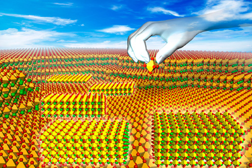
Atomically Thin Perovskites Boost for Future Electronics
- 前の記事
- 一覧に戻る
- 次の記事
2017.12.26
WPI-MANA has developed the world's highest performance dielectric nanofilms using atomically thin perovskites. This technology may revolutionize the next-generation of electronics.
This research was conducted by a WPI-MANA research group led by Principal Investigator Minoru Osada and Director Takayoshi Sasaki of WPI-MANA at NIMS.
Electronic devices are getting smaller all the time, but there is a limit to how small they can get using current materials and technology. High-κ dielectric materials may be the key for developing electronic devices of the future.
Minoru Osada and colleagues created high-performance dielectric nanofilms using 2D perovskite nanosheets (Ca2Nam−3NbmO3m+1; m = 3–6) as building blocks. Perovskite oxides offer tremendous potential for controlling their rich variety of electronic properties including high-κ dielectric and ferroelectric.
The researchers demonstrated the targeted synthesis of nanofilms composed of 2D perovskite nanosheets in a unit-cell-upon-unit-cell manner. In this unique system, perovskite nanosheets enable precise control over the thickness of the perovskite layers in increments of ~0.4 nm (one perovskite unit) by changing m, and such atomic layer engineering enhances the high-κ dielectric response and local ferroelectric instability. The m = 6 member (Ca2Na3Nb6O19) attained the highest dielectric constant, εr = ~470, ever realized in all known dielectrics in the ultrathin region of less than 10 nm.
Perovskite nanosheets are of technological importance for exploring high-κ dielectrics in 2D materials, which have great potential in electronic applications such as memories, capacitors, and gate devices. Notably, perovskite nanosheets afforded high capacitances by relying on high-κ values at a molecular thickness. Ca2Na3Nb6O19 exhibited an unprecedented capacitance density of approximately 203 μF cm-2, which is about three orders of magnitude greater than that of currently available ceramic condensers, opening a route to ultra-scaled high-density capacitors.
These results provide a strategy for achieving 2D high-κ dielectrics/ferroelectrics for use in ultra-scaled electronics and post-graphene technology.
Reference
"Atomic Layer Engineering of High‑κ Ferroelectricity in 2D Perovskites"
Bao-Wen Li, Minoru Osada, Yoon-Hyun Kim, Yasuo Ebina, Kosho Akatsuka, and Takayoshi Sasaki
Journal : J. Am. Chem. Soc. 139, 10868−10874 (2017)
DOI : 10.1021/jacs.7b05665
Bao-Wen Li, Minoru Osada, Yoon-Hyun Kim, Yasuo Ebina, Kosho Akatsuka, and Takayoshi Sasaki
Journal : J. Am. Chem. Soc. 139, 10868−10874 (2017)
DOI : 10.1021/jacs.7b05665
Affiliations
International Center for Materials Nanoarchitectonics (WPI-MANA), National Institute for Materials Science (NIMS), Namiki 1-1, Tsukuba, Ibaraki 305-0044, Japan
Contact information
ナノアーキテクトニクス材料研究センター (MANA)
〒305-0044 茨城県つくば市並木1-1
TEL: 029-860-4710
E-mail: mana-pr=ml.nims.go.jp([ = ] → [ @ ] )
TEL: 029-860-4710
E-mail: mana-pr=ml.nims.go.jp([ = ] → [ @ ] )