


Researches
Our group has been working on a variety of researches as follow.
- Superconducting atomic layers at surfaces and interfaces
- Diamond field-effect transistors (FET)
- Surface characterization with laser-based two-photon angle resolved photoemission spectroscopy
- LaB6 electron sources with passivated with hBN atomic layers
1) The discovery of superconducting surface atomic-layer materials
It is possible to create two-dimensional (2D) electron systems with high carrier densities at the surface/interface of semiconductors and insulators using surface adsorbates, charge transfer, and electric-field effect, etc. The search for superconductivity in kind of ideal 2D systems is an fundamental and attractive field of research.
We have created highly crystalline indium atomic layers on silicon substrates and, for the first time, obtained direct evidence of superconducting transition in atomic layers by measuring the zero resistance at low temperatures. The obtained transition temperature (Tc ~ 3 K) is nearly equal to the bulk value of indium, of which surface atomic layers are made. Furthermore, supercurrents can run over a macroscopic distance and the critical density is as high as 5.8×10⁵ A/cm2. This is surprising considering that the supercurrents are spatially confined within an atomic-scale thickness and numerous atomic steps on a surface could hinder their flows.
Recently, 2D superconductors have been discovered in various types of surface and interfaces, including one with a very high Tc. These studies constitute a new research field of 2D superconductors with atomic-scale thickness
References
- Takashi Uchihashi et al., "Macroscopic Superconducting Current through a Silicon Surface Reconstruction with Indium Adatoms: Si(111)-(√7×√3)-In", Phys. Rev. Lett. 107, 207001 (2011) [highlighted as an Editor's Suggestion and a Viewpoint in Physics].
- Takashi Uchihashi, "Two-dimensional Superconductors with Atomic-scale Thicknesses", Supercond. Sci. Technol. 30, 013002(1-37) (2017) [Topical Review].
- Takashi Uchihashi, "Two-Dimensional Superconductors - Phenomena at Surfaces/Interfaces and Atomic Layers" (KYORITSU SHUPPAN) (2022) (in Japanese).
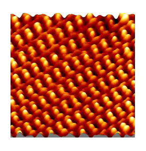
STM image of an indium atomic layer on a silicon surface (Si(111)-(√7×√3)-In).
-
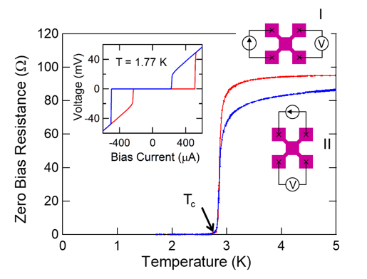
Superconducting transition of the Si(111)-(√7×√3)-In revealed by electron transport measurements.
- STM image of an indium atomic layer on a silicon surface (Si(111)-(√7×√3)-In).
- Superconducting transition of the Si(111)-(√7×√3)-In revealed by electron transport measurements.
2) STM imaging of an indium atomic layer on a silicon surface (Si(111)-(√7×√3)-In).
When magnetic field is applied to a superconducting surface, supercurrent vortices are created by the penetration of the field. Using a scanning tunneling microscope (STM), we have found that vortices trapped at atomic steps are strongly deformed and that the superconducting state is recovered at the vortex core that should have normal-like states. This means that atomic steps can work as Josephson junctions. Such vortices running along Josephson junctions are called Josephson vortices.
The Josephson vortices are known to play important roles in high-Tc superconductors, but this is the first time to directly observe their electronic states. This finding is also important in terms of application, because Josephson junctions are the most basic component for superconducting devices. (This work is based on collaborations with the groups of Y. Hasegawa at ISSP, Tokyo University and X. Hu at NIMS.)
References- Shunsuke Yoshizawa et al., "Imaging Josephson Vortices on the Surface Superconductor Si(111)-(√7×√3)-In using a Scanning Tunneling Microscope", Phys. Rev. Lett. 113, 247004 (2014) [highlighted as an Editor's Suggestion and a Synopsis in Physics].
- Yudai Sato et al., ”Squeezed Abrikosov-Josephson vortex in atomic-layer superconductors formed on vicinal substrates”, Phys. Rev. Lett. 130, 106002(1-6) (2023).
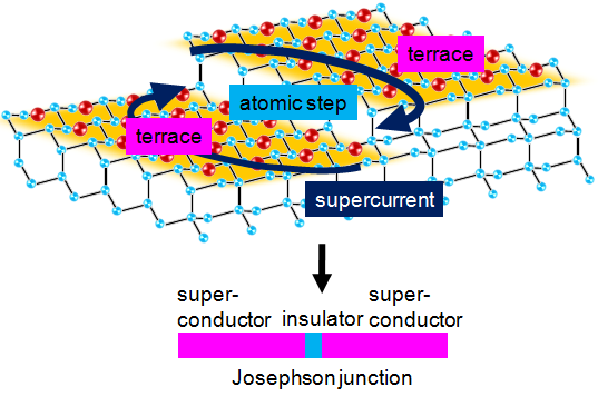
Schematic diagram of an atomic-layer superconductor and an atomic step. The arrow indicates that supercurrents run over the step to form a vortex.
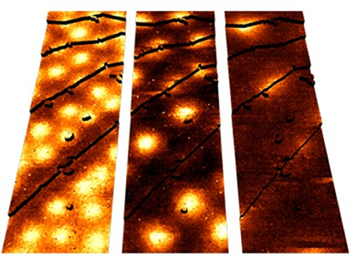
Superconducting vortices imaged with an STM. (B = 0.08 T, 0.04 T, 0.00 T from left to right.) The bright features correspond to the cores of the vortices. Josephson vortices trapped at atomic steps are visible in the right image.
- Schematic diagram of an atomic-layer superconductor and an atomic step. The arrow indicates that supercurrents run over the step to form a vortex.
- Superconducting vortices imaged with an STM. (B = 0.08 T, 0.04 T, 0.00 T from left to right.) The bright features correspond to the cores of the vortices. Josephson vortices trapped at atomic steps are visible in the right image.
3) Giant critical magnetic fields caused by the Rashba-type spin-orbit coupling
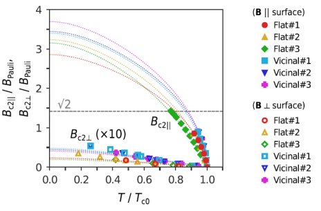
Since the space-inversion symmetry is broken at the solid state surfaces (electrostatic potentials are different between the vacuum and substrate sides), the Rashba-type spin-orbit coupling (SOC) generally appears and induces the spin splitting of energy bands. We have successfully observed Fermi surface splitting of indium atomic layers on silicon using laser-based angle-resolved photoemission spectroscopy (ARPES). We have also measured the critical magnetic fields (BC2) of the sample at low temperatures and found that BC2 in the in-plane direction is anomalously enhances beyond the Paul limit, the standard theoretical prediction for critical field. This is due to extremely short spin flipping times, which are caused by the Rashba-type SOC and the locking relation between of spin and electron motion. We have proposed such dynamic mechanism of spin-momentum locking and successfully obtained strong evidence for it through detailed analysis of electron transport measurements.
Superconductors robust against magnetic field is practically important. It has also been proposed to create topological superconductors and Majorana states by combining Rashba-type SOC, strong magnetic field, and superconductivity. Our finding will be a basis for such future studies. (This work is based on collaborations with the groups of K. Sakamoto at Osaka University and K. Yaji at NIMS.)
References- S. Yoshizawa et al., “Atomic-layer Rashba-type superconductor protected by dynamic spin-momentum locking”, Nat. Commun. 12, 1462 (2021).
- T. Kobayashi et al., “Orbital angular momentum induced spin polarization of 2D metallic bands”, Phys. Rev. Lett. 125, 176401 (2020).
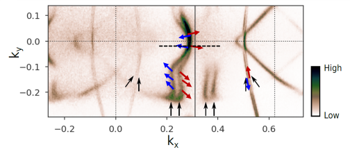
(Top) Fermi surface of an indium atomic layer superconductor obtained by lased-based ARPES. The red and blue arrows indicate the spin polarization directions.
(Bottom) Temperature dependence of in-plane and out-of-plane critical magnetic fields. The magnetic field and temperature are normalized by the Pauli limit (BPauli = 5.5 – 5.8 T) and superconducting transition temperature (Tc0 = 2.97 - 3.14 K), respectively.