Imaging-type spin-resolved photoemission microscopy
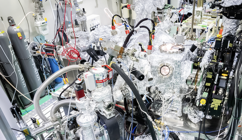
This microscopic spin-resolved photoemission spectroscopy system is currently in operation at the Sakura site. It employs a photoelectron momentum microscope as the electron analyzer and a 10.9 eV vacuum-ultraviolet laser as the excitation source. Spin-resolved photoemission measurements can be performed in both real and momentum space. In real-space mode, spatial resolutions of 30 nm for spin-integrated measurements and 400 nm for spin-resolved measurements have been achieved. We have also successfully developed Japan’s first imaging-type spin detector, which improves the data acquisition efficiency by a factor of 10,000 compared with conventional spin-resolved photoemission spectroscopy.
Soft-X-ray complete operando photoemission ultramicroscopy "SCORPIUS"
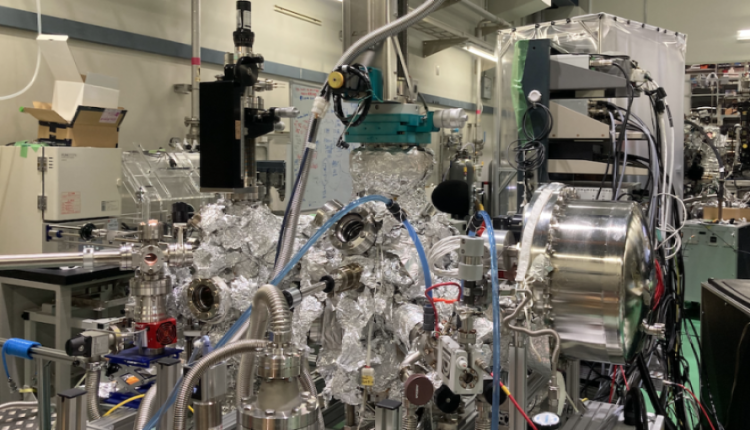
The Soft-X-ray Complete OpeRando PhotoemIssion UltramicroScopy (SCORPIUS) system has been commissioned at BL07U of NanoTerasu, a 3 GeV high-brilliance synchrotron radiation facility. SCORPIUS enables visualization of the electronic and spin states of materials and devices, from equilibrium conditions to actual operating environments.
Standard photoemission spectroscopy machine
This is a photoemission spectroscopy system equipped with an SES100 analyzer, currently operating at the Sakura site. An X-ray source and a helium discharge lamp are installed as excitation sources, enabling both XPS and UPS measurements.
AFM and Raman analysis

Integrated AFM-Raman System“XploRA Nano”
This system combines atomic force microscopy (AFM) with micro-Raman spectroscopy. It enables surface morphology and local physical-property characterization by AFM together with Raman spectroscopic analysis of crystal structures and vibrational properties at the same sample location. The system also supports tip-enhanced Raman spectroscopy (TERS) for nanoscale spectroscopic measurements and operando measurements under external stimuli such as applied voltage.
Operand micro Raman spectroscopy
A piezo-driven independent four-probe stage has been integrated into our micro-Raman spectroscopy system. This setup enables operando Raman analysis of microfabricated devices, as well as simultaneous transport and spectroscopic measurements of nanomaterials without the need for electrode fabrication. We also perform machine-learning-based analysis of spectral data.
SEM and Transport measurements

Four-Tip Scanning Electron Microscope "4tip-SEM"
The 4tip-SEM is equipped with four independently movable microprobes inside a scanning electron microscope (SEM). It enables local electrical transport measurements of microscale samples and in-situ observation of changes induced by applied electric fields while observing the sample surface and probe positions by SEM. Thin films grown in an adjacent molecular beam epitaxy (MBE) system can also be transferred without exposure to air for SEM observation and electrical transport measurements.





.png)