Welcome to the website of
Minari Group -Printed Electronics-!
National Institute for Materials Science (NIMS)
Research
Outline
Printed electronics is a technology that allows bottom-up fabrication of electronic devices from functional inks using printing techniques. Large-scale, low-cost production of printed electronic devices is now expected because of the recent development of novel inks and printing techniques. We are pursuing the fabrication of printed electronics by developing novel patterning methods using different functional inks. In particular, we focus on organic field-effect transistors (OFETs) as key devices in next-generation flexible electronics. The physics of charge injection and transport in OFETs is also studied.
Fully-printed organic field-effect transistor arrays
Printed electronics has become a field of global research because it offers the possibility of low-cost fabrication of semiconductor devices. In order to minimize fabrication costs, it is essential to form all layers in devices by printing under an ambient atmosphere. We have successfully fabricated flexible OFET arrays by employing printing methods for all device layers, and an average mobility of 8 cm2/(V×s) has been achieved (Fig. 1). Since this is ten times higher than the value for conventional a-Si TFTs, and is comparable to that for IGZO TFTs, it highlights the practical potential of printed devices.
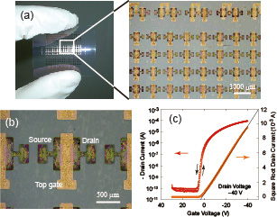
Fig. 1 (a) Fully-printed OFET devices fabricated on a plastic substrate. (b) Optical micrograph of an individual device. (c) Typical I?V characteristics for the OFET devices.
Contact resistance in organic field-effect transistors
Typically, the contact resistance (RC) in OFETs is reported to be 1-100 kΩ×cm, which is much higher than that for inorganic semiconductor devices. This leads to a lower mobility and a poorer subthreshold slope, in addition to a shift in the threshold voltage (VT). The high RC has been found to be due to a combination of the resistance of the path from the electrode to the channel (Rbulk) and that associated with the metal/organic semiconductor interface (Rint). To fabricate OFETs with lower RC values, we introduced a dopant at the metal/organic semiconductor interface to reduce Rint, and employed a top-gate structure to eliminate Rbulk (Fig. 2).
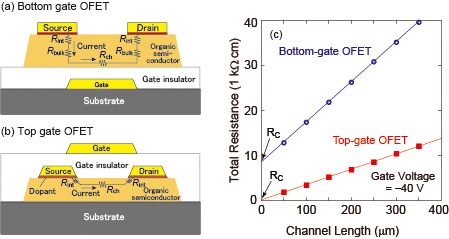
Fig. 2 Schematic illustrations of OFETs with bottom-gate (a) and top-gate (b) structures. (c) Contact resistance for bottom-gate and top-gate OFETs, determined by the transfer length method (TLM).
Bias stress effect in organic field-effect transistors
A critical requirement for practical use of OFETs is stability against the bias-stress (BS) effect, in which a shift in VT occurs under continuous application of a gate voltage (VG). The BS effect is thought to be the result of charge trapping at the semiconductor/insulator or the metal/organic semiconductor interface. However, the precise mechanism has still not been clarified. We are currently fabricating polycrystalline and single-crystal OFET devices in order to reveal the origin of the BS effect.
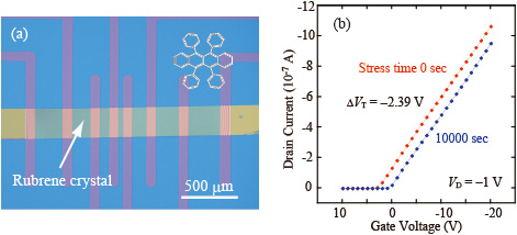
Fig. 3 (a) Organic single-crystal transistors of rubrene. (b) Typical I?V characteristics of single-crystal OFETs before (0 sec) and after applying a VG of -20 V for 10000 sec.
Analysis of transient response in organic field-effect transistors
OFETs exhibit a transient state after a step gate voltage is applied. Analysis of this transient state is essential because OFET devices may be driven by AC voltages in practical applications. The relationship between the charge injection process and the transient response is particularly important because of the large RC in OFETs. For example, an OFET with Cu electrodes shows a better AC response than one with Au electrodes (Fig. 4).
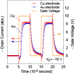
Fig. 4 Transient response of pentacene OFETs with Cu or Au electrodes.