Sensor Chemistry Group
The development of high-controllable chemistry to realize novel sensor devices.
Group Top HOME JAPANESE NIMS TOP
Research
Member
Publication
Contact
Link
 
Research

Chemical sensing function composed mainly of tow factors.  One is “receptor function” that means a recognition function of a specific chemical species. The other, “ transducer function” that transducer information of chemical species to some physical signal.  In order to provide intelligence to sensor materials, we are thinking, clarifying the basics of these functions is essential. We are developing procedures of searching sensor functions, creating new thin film materials having potential of high response.  Multi sensor devices are believed to be effective to realize the intelligent sensor system.  To realize this kind of sensor system, we are synthesizing nano-particles via aqueous solution, developing patterning process of these particles.  Furthermore, sensors with carbon nano-tubes are developed.  


Searching new chemical sensor materials with a combinatorial ion implantation and SPR phenomenon.

Doping of different elements with host materials is effective in improving the sensor function. We are developing a procedure of rapidly searching sensor materials using a combinatorial ion implantation tool that had been developed in our group. Using this equipment, wide rang doping test with wide range of additive concentration is possible form ppb to % order.

Schematic diagram of combinatorial ion implantation
 
As for combinatorial-searching of new sensor functions, we are studying on the surface plasmon resonance that will be expected to be applied sensor searching. Although this method is mainly for searching of receptor function in sensor devices, it is believed to be applied to study on transducer function of sensor through fundamental understanding of this phenomenon.
 

Schematic drawing of SPR

 
Surface Plasmon:
The electron charges on metal boundary can perform coherent fluctuations which are called surface plasma oscillations.
Evanescent Wave:
Evanescent wave is appropriate because the intensity of evanescent waves decays exponentially with distance from the interface at which they are formed. Evanescent waves are formed when sinusoidal waves are (internally) reflected off an interface at an angle greater than the critical angle so that total internal reflection occurs.
SPR
If the wavenumbers of above mentioned lights corresponding with each other, intensity of reflected wave is reducing. This resonance phenomenon is greatly affected by adsorptive materials on surface.
 
Detecting of sucrose with SPR in ZnO/Au hetero thin film system.

Thin film synthesis with ion/molecular beams.

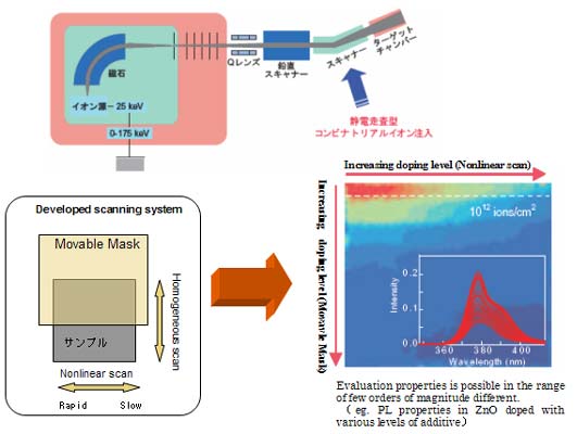
The main research field is the growth of single-crystalline thin films using molecular beams and/or ion beams generated by the Accelerator-Linked- Instrument for Synthesis and Analysis, ALISA. (see following figure)

A single-crystalline film can demonstrate the intrinsic properties. And the model system constructed with the single-crystalline films is useful for probing and understanding the interaction between the material and the surrounding environment. The process adopted here is a non-equilibrium one, which has potential for realizing novel morphology, composition, structure, etc. leading to new properties and/or materials.
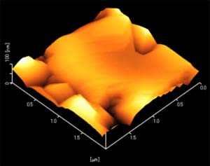
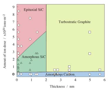
Figures, which are the results obtained using the ALISA, are a RHEED pattern of the epitaxial ZnO thin film grown on ZrB2 at room temperature, a AFM topography of Pt single-crystalline grains on silica glass grown through ion-beam process, and a phase diagram at room temperature in Si-C system by ion-beam induced crystallization.


RHEED pattern of ZnO film grown on ZrB2


 AFM image of Pt film on SiO2 glas

 
Phase relation in Si-C system at room temperature induced by ion-beam irradiation
 

Aqueous solution processes for ceramics

Aqueous solution processes enable us to prepare ceramics having various shapes at low temperatures.  In order to make higher sensitive and smaller ceramic gas sensor, we try to develop novel processes for semiconducting oxide ceramics such as ZnO.

 
Fig. Micropatterns of ZnO prepared by an aqueous solution process
 
Page Top Page Top

Copyright (C) NIMS. All rights reserved. Never reproduce or republicate without written permission.