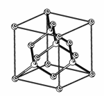
Hexagonal Boron Nitride as a new Far UV luminous material
We clarified for the first time that hexagonal boron nitride, which is used as insulation and heat- resistant materials, becomes a highly effective light-emitting device that emits light in the far ultraviolet region at room temperature. We obtained a highly pure monocrystal by growing a purified raw material in a mixture solvent composed of barium – boron nitride under high-temperature and high-pressure using a 30,000 ton high-pressure apparatus. Using this crystal, the group obtained very strong luminescence with a wavelength of 215 nm (nano: 1/billion).
This is the first semiconductor light-emitting device in the far ultraviolet region near the wavelength of 200 nm. The possibility of application to light-emitting devices such as semiconductor laser devices has been demonstrated through experiments of electron beam irradiation.
In future, by incorporating this device with electron beam sources such as carbon nanotube and diamond, compact ultraviolet lasers or strong ultraviolet ray sources will be realized. Various applications such as light sources for decomposing environmental pollutants, high integration of DVD light recording devices, and excitation light sources for fluorescent lamps are expected.
New developments of hBN applications – Use of hBN substrate for graphene increases graphene mobility
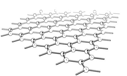
Graphene – atomic layer(s) of graphite is one of famous materials for its exceptional electronic and thermal properties. It shows various interesting phenomena in physics, such as electron conduction as Dirac Fermion and fractional quantum Hall effect, and is one of promising materials for its applications for Ultra high speed FET, monoelectron transistor, spin related device and so on.
However, practically, as can be seen in the use of conventional SiO2 substrates, graphene cannot show its intrinsic properties including ultra high mobility due to its undulation and/or impurity scattering originated by SiO2 substrates.
Instead of conventional SiO2 substrates, the use of h-BN substrates solved the problems. The crystal structure of h-BN is smiler to that of graphite. The 2 dimensional layer composed of boron and nitrogen atoms in sp2 bonding, has no dangling bond in the out of plane direction. In addition, h-BN is one of the wide band gap materials, thus, it can compose layers of insulation and does not disturb the graphite two-dimensional electric conduction.
By using hBN for the substrate of graphene, the electrical conduction properties of the graphene improved significantly, and its mobility reached almost one-order higher than that of the conventional SiO2 substrate device and quantum electronic correlation effects such as fractional quantum Hall effect rushed to observed in the graphene layers on the hBN substrate .
C. R. Dean, A. F. Young, I. Meric, C. Lee, L. Wang, S. Sorgenfrei, K. Watanabe, T. Taniguchi, P. Kim, K. L. Shepard, and J. Hone, “Boron nitride substrates for high-quality graphene electronics,” Nature Nanotechnology. 5 722-726 (2010).
はじめに (Japanese)
MEMBERS