|
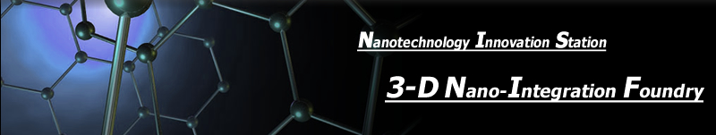
Electron beam lithography system |
| |
|
Product |
ELS-7000 |
Manufacturer |
Elionics |
Capabilities |
Electron beam gun: ZrO/W thermal field emission type
Minimum line width: 8nm @ 100kV
Maximun acceleration voltage: 100kV (25kV step)
Substrate sizes: 5mmx5mm chip ~ 6" wafer
Stitching accuracy: less than 40nm
Superposing accuracy: less than 40nm |
|
| |
【Applications】 |
|
|
|
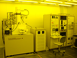
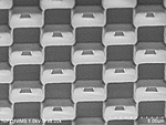
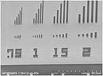
Φ200 nm hole array |
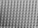
100 nm line patterns
(bilayer resist) |
|
|
|
|
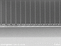
Laser lithography system |
| |
|
Product |
DL-1000 |
Manufacturer |
Nanosystem Solutions, Inc. |
Capabilities |
Light source: semiconductor laser ( 405nm )
Light intensity: 300mW/cm2
Positioning accuracy: less than ±1um
Superposing accuracy: less than ±1um
Maximum wafer size: 4" wafer
Maximum mask size: 4"square (thickness 2.3mm)
|
|
| |
【Applications】 |
|
|
|
3 um square pattern
(bilayer resist) |
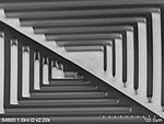
Φ5 um pillar Array
(epoxy-based negative photoresist) |
|
|
|
|
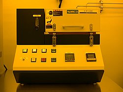
Mask aligner |
| |
|
Product |
SUSS MA6 BSA |
Manufacturer |
SUSS Microtec |
Capabilities |
Exposure mode: proximity, soft, hard, and vacuum contact
Wavelength: 350 ~ 450nm
Resolution: 0.5um
Top side alignment accuracy: 0.5um
Bottom side alignment accuracy: 1.0um
Maximum wafer size: 6" wafer
|
|
| |
【Applications】 |
|
|
|
Rectangular pattern
(negative photoresist) |
L/S pattern
(negative photoresist) |
|
|
|
|
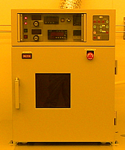
Plasma asher |
| |
|
Product |
PB-600 |
Manufacturer |
Yamato Scientific. Co., Ltd. |
Capabilities |
Plasma mode: DC
High frequency output: 0 ~ 600W (continuous variable)
Reactive gas: O2, CF4
Substrate sizes: Max 6” wafer
Timer: 1sec ~ 9h59m59s |
|
|
UV ozone cleaner |
| |
|
Product |
UV-1 |
Manufacturer |
SAMCO International Inc. |
Capabilities |
UV lamp: wavelength 253.7nm and 184.9nm (110W)
Substrate sizes: Max 8” wafer
Stage temperature: RT ~ Max 300 degrees C
Timer: 0 ~ 99h99m |
|
| |
|
|
|