Joint Workshop LANL/NIMS Quantum and Functional Materials and MANA International Symposium 2024
Quantum Materials - 08
Title
Neuromorphic operations based on a floating-gate-type organic antiambipolar transistor

Authors
Yuho Yamamoto
Affiliations
URL
https://www.nims.go.jp/mana/jp/research/b5alu400000005bh.html
yamamoto.yuuho@nims.go.jp
Abstract
An antiambipolar transistor (AAT) has a PN junction in the transistor channel and exhibits a Λ-shaped transfer curve
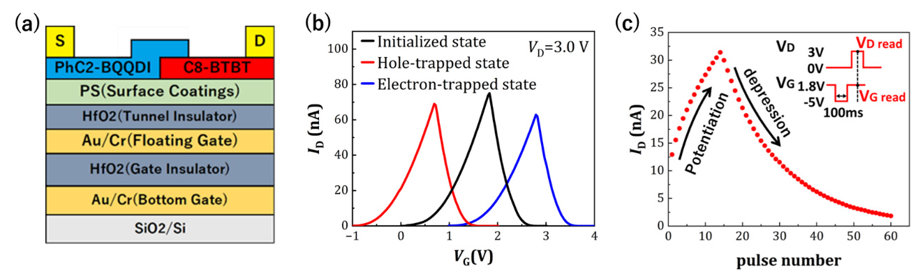
The device structure of the FG-AAT is shown in Fig. (a), where C8-BTBT (16 nm) and PhC2-BQQDI (8 nm) films were used as p-type and n-type transistor channels, respectively. Additionally, a Au/Cr film acted as the floating gate. A 10 nm-thick polystyrene (PS) film was formed as the surface coating layer. Fig. (b) shows the drain current–gate voltage (ID–VG) characteristics of the FG-AAT at the initial (black), hole-trapped (red), and electron-trapped (blue) states. In the initial state, a Λ-shaped transfer curve was observed with a peak voltage (Vpeak) of 1.8 V. The Vpeak was shifted from 1.8 V to 2.8 V (blue line) by applying a positive pulse voltage (VG = 5 V, width = 10 s) due to the electron accumulation in FG. Conversely, a negative pulse voltage (VG = –5 V, width = 10 s) decreased Vpeak from 1.8 V to 0.7 V owing to the hole accumulation in FG. The overall Vpeak shift reached 2.1 V. This feature was then applied to neuromorphic device operations. When a negative pulse voltage (VG = –5 V, width = 100 ms) was applied, ID increased, indicating long-term potentiation. Significantly, ID was transited from increase to decrease by applying the negative pulse voltages consistently. This operation coincides with the long-term depression (Fig. (c)). Usually, such synaptic plasticity is attained by applying the pulse voltage with the opposite polarity. However, Λ-shaped transfer curve induced in AAT enables the continuous change from potentiation to depression even with the same pulse voltages. This finding has the potential to develop reconfigurable synaptic operations using FG-AATs.
Reference
- K. Kobashi et al., Adv. Electron. Mater. 3(8), 1700106, (2017).. DOI 10.1002/aelm.201700106
- R. Hayakawa et al., Adv. Mater. 34(15), 2109491, (2022). DOI 10.1002/adma.202109491
- R. Hayakawa et al., Nano Lett. 23(17), 8339-8347, (2023). DOI 10.1021/acs.nanolett.3c02726